41
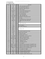
1
CLK
O
CLOCK output for MAIN, FRONT C.B.
2
DATA
O
DATA output for MAIN, FRONT C.B.
3
STB (M)
O
Data latch strobe output for MAIN C.B.
4
_________
O-LED
O
______
LED ON/OFF output.
5
STB (SHIFT)
O
Latch strobe output for FRONT shift register.
6
_______________
RYM-CS
O
Latch strobe output for RHYTHM IC.
7
PLL-CE
O
PLL IC chip enable output.
8
GEQ-CE
O
GEQ IC chip enable output.
9
_____________________
O-CLK SHIFT
O
TUNER CLOCK SHIFT output.
10
I-TM-BASE
I
REFERENCE CLOCK input for timer watch.
11
______________
RESET
I
Reset input.
12
I-DISH
I
CD turntable photo sensor A/D converter input.
13
__________________
I-HP-MUTE
I
Headphone input for MUTE by PROLOGIC.
14
VSS 1
—
GND.
15
CF 1
—
9.43MHz oscillator circuit.
16
CF 2
—
17
VDD 1
—
Power supply input.
18
___________
I-HOLD
I
Power failure detection input.
19
I-KEY-1
I
20
I-KEY-2
I
KEY input. (A/D)
21
I-KEY-3
I
22
I-CD SW
I
CD mechanical switch A/D converter input.
23
I-RTVR
I
Rotary volume A/D level input.
24
I-JOG
I
JOG dial A/D level input.
25
I-MIC
I
Microphone input for AUTO VF.
26
_______
I-TU-SIG/MS
I
Tuner signal and deck music sensor signal input.
27
I-SPEANA
I
A/D input for spectrum analyzer display.
28
I-WRQ/RDS-CLK
I
CD WRQ input/Tuner RDS clock input.
29
__________
I-RMC
I
System remote control signal input.
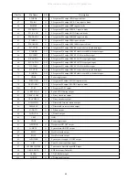
30-42
G13-G1
O
FL GRID output G13-G1.
43-45
P36-P34
O
FL SEGMENT output P36-P34.
46
VDD3
—
Power supply input.
47
SPEANA-A/P33
O
Spectrum analyzer band switching ouput A/FL segment P33 output.
48
SPEANA-B/P32
O
Spectrum analyzer band switching ouput B/FL segment P32 output.
49
SPEANA-C/P31
O
Spectrum analyzer band switching ouput C/FL segment P31 output.
50
_____________
RHYM/P30
I/O
RHYTHM input to diode/FL segment P30 output.
51
–VP
—
Power supply input for FL display.
52
P29/AM-ST
O
FL segment P29 output/AM-ST input to diode.
53
P28/LW
O
FL segment P28 output/LW input to diode.
54
P27/SW
I/O
FL segment P27 output/SW input to diode.
55
P26/FM1
O
FL segment P26 output/FM1 (OIRT) input to diode.
Description
Pin No.
Pin Name
I/O
IC DESCRIPTION
IC, LC876572V-5L10
All manuals and user guides at all-guides.com
Summary of Contents for NSX-L980
Page 12: ...14 13 BLOCK DIAGRAM 1 MAIN All manuals and user guides at all guides com ...
Page 13: ...15 BLOCK DIAGRAM 2 TUNER All manuals and user guides at all guides com ...
Page 15: ...17 SCHEMATIC DIAGRAM 1 TUNER 18 All manuals and user guides at all guides com ...
Page 17: ...21 SCHEMATIC DIAGRAM 2 DECK 22 All manuals and user guides at all guides com ...
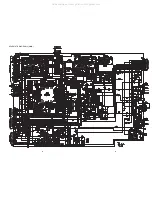
Page 19: ...25 SCHEMATIC DIAGRAM 4 MAIN 26 All manuals and user guides at all guides com ...
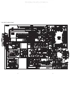
Page 20: ...27 SCHEMATIC DIAGRAM 5 FRONT 28 S19 All manuals and user guides at all guides com ...
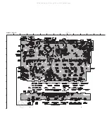
Page 22: ...31 SCHEMATIC DIAGRAM 6 AMP 32 All manuals and user guides at all guides com ...
Page 25: ...35 SCHEMATIC DIAGRAM 7 PT All manuals and user guides at all guides com ...
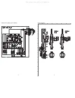
Page 28: ...40 39 FL GRID ASSIGNMENT ANODE CONNECTION All manuals and user guides at all guides com ...
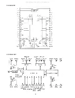
Page 32: ...44 IC M62449FP IC M65847AFP All manuals and user guides at all guides com ...
Page 33: ...45 IC LA1837NL IC LC72131D All manuals and user guides at all guides com ...


