background image

30

29

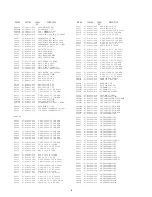
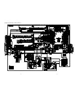
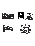
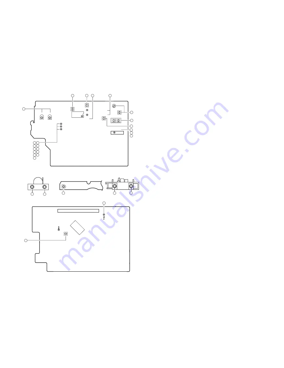
ADJUSTMENT

 11

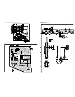
DECK-2 R/P HEAD

FWD

FRONT  C.B 

IC201

FL401

GND

TP7

16

16

L331

C326

1

R268

+

30

11

REV

FWD

DECK-1 P HEAD 

11

10

SFR1

DECK  C.B

 11

REV

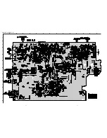
MAIN  C.B

L951

SFR451 SFR452

L801

TP2 (CLK)

TP4  (DC BALANCE)

GND

TP8 (RCH)

TP9 (LCH)

10

 2

L802

L942

L941

TC942

9

5

TP1 (VT)

(3/3) (1/3)

FFE831

TP3  (DC BALANCE)

8

1

3

4

3

5

6

7

8

9

11

12

13

14

15

9

6

14

IC801

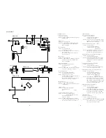
< TUNER SECTION >
1. Clock frequency Check

Settings : • Test point : TP2
Method : Set to AM 1602kHz and check that the test point is

2052kHz 

±

 45Hz.

2. MW VT Check

Settings : • Test point : TP1 (VT)
Method : Set to MW 1602kHz, 531kHz and check that the

test point is less than 8.0V (1602kHz) and more
than 0.6V (531kHz).

3. LW VT Adjustment

Settings : • Test point : TP1 (VT)

• Adjustment location: L942

Method : Set to LW 144kHz and adjust L942 so that the test

point is 1.3V 

±

 0.05V.

Then set to LW 290kHz and check that the test
point is less than 8.0V.

4. FM VT Check

Settings : • Test point : TP1 (VT)
Method : Set to FM 87.5MHz, 108.0MHz and check that the

test point is more than 0.5V (87.5MHz) and less
than 8.0V (108.0MHz).

5. MW Tracking Adjustment

Settings : • Test point : TP8(Lch), TP9(Rch)

• Adjustment location :
L951(1/3) ...................................... 999kHz

Method : Set to MW 999kHz and adjust L951(1/3) so that the

level at the test point becomes maximum.

6. LW Tracking Adjustment

Settings : • Test point : TP8(Lch), TP9(Rch)

• Adjustment location : L941, TC942

Method : Set up TC942 to center position.

Set to LW 144kHz and adjust L941 so that the level
at test point becomes maximum.
Then set to LW 290kHz and adjust TC942 so that
the level at test point becomes maximum.

7. FM Tracking Check

Settings : • Test point : TP8(Lch), TP9(Rch)
Method : Set to FM 98.0MHz and check that the test point is

less than 13dB

µ

V.

8. AM IF Adjustment

Settings : • Test point : TP8(Lch), TP9(Rch)

• Adjustment location :
L802 ............................................. 999kHz

9. DC Balance / Mono Distortion Adjustment

Settings : • Test point : TP3, TP4 (DC Balance)

: TP8(Lch), TP9(Rch) (Distortion)

• Adjustment location : L801
• Input level : 60dB

µ

V

Method : Set to FM 98.0MHz and adjust L801 so that the

voltage between TP3 and TP4 becomes 0V 

±

 0.3V.

Next, check that the distortion is less than 1.3%.

< DECK SECTION >
10. Tape Speed Adjustment (DECK 2)

Settings : • Test tape : TTA–100

• Test point : TP8(Lch), TP9(Rch)
• Adjustment location : SFR1

Method : Play back the test tape and adjust SFR1 so that the

frequency counter reads 3000Hz 

±

 5Hz and 

±

45Hz

(REV) with respect to forward speed.

11. Head Azimuth Adjustment (DECK 1, DECK 2)

Settings : • Test tape : TTA–330

• Test point : TP8(Lch), TP9(Rch)
• Adjustment location : Head azimuth

          adjustment screw

Method : Play back (FWD) the 8kHz signal of the test tape

and adjust screw so that the output becomes
maximum. Next, perform on REV PLAY mode.

12. PB Frequency Response Check (DECK 1, DECK 2)

Settings : • Test tape : TTA–300

• Test point :TP8(Lch), TP9(Rch)

Method : Play back the 315Hz and 8kHz signals of the test

tape and check that the output ratio of the 8kHz
signal with respect to that of the 315Hz signal is
within 5dB.

13. PB Sensitivity Check (DECK 1, DECK 2)

Settings : • Test tape : TTA–200

• Test point : TP8(Lch), TP9(Rch)

Method : Play back the test tape and check that the output

level of the test point is 140mV 

±

 3dB.

14. REC/PB Frequency Response Adjustment (DECK 2)

Settings : • Test tape : TTA–602

• Test point : TP8(Lch), TP9(Rch)
• Input signal : 1kHz / 8kHz (LINE IN)
• Adjustment location : SFR451 (Lch)

SFR452 (Rch)

Method : Apply a 1kHz signal and REC mode. Then adjust

OSC attenuator so that the output level at the TP8,
TP9 becomes -20VU. Record and play back the
1kHz and 8kHz signals and adjust SFRs so that the
output of the 8kHz signals becomes 0dB 

±

 0.5dB

with respect to that of the 1kHz signal.

15. REC/PB Sensitivity Check (DECK 2)

Settings : • Test tape : TTA–602

• Test point : TP8(Lch), TP9(Rch)
• Input signal : 1kHz (LINE IN)

Method : Apply a 1kHz signal and REC mode. Then adjust

OSC attenuator so that the output level at TP8, TP9
becomes 0VU. Record and play back the 1kHz
signals and check that the output is –2dB 

±

 3.0dB.

< FRONT SECTION >
16.

µ

-CON OSC Adjustment

Settings : • Test point : TP7 and GND

• Adjustment location : L331

Method : Insert AC plug while pressing POWER and TUNER

function keys. Adjust L331 so that the frequency
atthe test point is 153.84Hz 

±

 0.15Hz.

Summary of Contents for NSX-BL44

Page 1: ...ANISM 6ZM 3 YPR2N DR6 BASIC CD MECHANISM AZG 1 ZA3RDM 44 46 BASIC CD MECHANISM AZG 1 YZA3RDM DR6 NSX BL44 NSX BL46 NSX DR6 EZ K G EZ EZ S M Code No 09 002 429 5N2 If requiring information about the CD mechanism see Service Manual of AZG 1 S M Code No 09 001 335 3NC SPEAKER SX NSZ53 NSX BL44 EZ K CX NBL44 SX NBL40 NSX BL46 EZ NSX DR6 EZ CX NDR6 SX NBL40 CX NBL46 SX NBL42 ...

Page 2: ...RS accept speakers of 6 ohms or more SURROUND SPEAKERS accept speakers of 8 ohms to 16 ohms PHONES stereo jack accepts headphones of 32 ohms or more SPECIFICATIONS Cassette deck section Track format 4 tracks 2 channels stereo Frequency response 50 Hz 15000 Hz Recording system AC bias Heads Deck 1 Playback head x 1 Deck 2 Recording playback head x 1 erase head x 1 Compact disc player section Laser ...

Page 3: ...fiés peut entraîner une dangereuse exposition aux radiations ADVARSEL Usynlig laserståling ved åbning når sikkerhedsafbrydereer ude af funktion Undgå udsættelse for stråling This Compact Disc player is classified as a CLASS 1 LASER product The CLASS 1 LASER PRODUCT label is located on the rear exterior This set employs laser Therefore be sure to follow carefully the instructions below when servici...

Page 4: ...ROCOMPUTER 1 Turn on the AC main power 2 Confirm that the main power is turned on and the HOLD terminal of the MICROCOMPUTER keeps the H level or not 3 When the HOLD terminal is L level the abnormality detection circuit is judged to be working correctly and the MICROCOMPUTER is judged to be good 1 Forced discharge of electrolytic capacitor of power supply block When repair is going to be attempted...

Page 5: ... the electrolytic capacitor C113 that is connected to VDD of the MICROCOMPUTER with tweezers 3 Connect the AC power cord again If the MICROCOMPUTER returns to the normal operation the MICROCOMPUTER is good Note The reference number or MICROCOMPUTER pin number of transistor Q110 and electrolytic capacitor C113 can change depending on the models Be sure to check the reference numbers on schematic di...

Page 6: ...010 380 080 CAP E 47 16 M 11L SME C0036 87 010 381 080 CAP E 330 16 M SME C0038 87 010 197 080 C CAP S 0 01 25 K B C2012 C0060 87 010 403 080 CAP E 3 3 50 M 11L SME C0061 87 010 260 080 CAP E 47 25 M 11L SME C0101 87 010 183 080 C CAP S 2700P 50 K B GRM C0102 87 010 183 080 C CAP S 2700P 50 K B GRM C0103 87 010 545 080 CAP E 0 22 50 M 11L SME C0104 87 010 545 080 CAP E 0 22 50 M 11L SME C0107 87 0...

Page 7: ...SME C0802 87 010 194 080 C CAP S 0 047 25 Z F C0803 87 010 198 080 C CAP S 0 022 25 K B C2012 C0804 87 010 263 080 CAP E 100 10 M 11L SME C0807 87 010 400 080 CAP E 0 47 50 M 11L SME C0808 87 010 401 080 CAP E 1 50 M 11L SME C0809 87 010 401 080 CAP E 1 50 M 11L SME C0810 87 010 196 080 C CAP S 0 1 25 Z F C2012 C0814 87 010 197 080 C CAP S 0 01 25 K B C2012 C0815 87 010 400 080 CAP E 0 47 50 M 11L...

Page 8: ...0 22 16 K W5R CM CB C0322 87 010 400 040 CAP E 0 47 50 M 11L SME C0325 87 A10 189 040 CAP E 220 10 M 5L C0326 87 A10 189 040 CAP E 220 10 M 5L C0332 87 010 178 080 C CAP S 1000P 50 K B C2012 C0334 87 010 312 080 C CAP S 15P 50 J CH GRM C0335 87 012 140 080 C CAP S 470P 50 J CH C0336 87 012 155 080 C CAP S 180P 50 J CH GRM C0339 87 012 156 080 C CAP S 220P 50 J CH GRM C0340 87 010 197 080 C CAP S 0...

Page 9: ...0 Z F C0031 87 010 403 040 CAP E 3 3 50 M 11L SME CN0001 87 A61 122 010 CONN 11P V TID A PT0001 8A NFJ 608 010 PT ANF 8 EZ 2 PT0002 8A NF8 662 010 PT SUB ANF 8 E RY0002 87 A91 418 010 RELAY AC12V G5PA 1 M T0001 87 A60 317 010 TERMINAL 1P MSC T0002 87 A60 317 010 TERMINAL 1P MSC REF NO PART NO KANRI DESCRIPTION NO 8 8 A Resistor Code Chip Resistor Part Coding Figure Value of resistor Chip resistor ...

Page 10: ...401 CMBT5551 CSD1306 KRA102S KRA107S KRC102S RT1N441C RT1P141C D G S 2SK360 G S D 2SK2158 E C B 2SA1981 2SC3331 2SC5343 CD1585 CSA952 CSC4115 KTA1266 KTC3198 E C B DTC114ES KTC3199 S D G 2SJ460 2SK2541 B C E 2SB1370 TRANSISTOR ILLUSTRATION ...

Page 11: ...12 11 FL HNA 11MM30 GRID ASSIGNMENT ANODE CONNECTION GRID ASSIGNMENT ANODE CONNECTION ...

Page 12: ...1 2 3 4 5 6 7 8 9 10 11 12 13 14 A B C D E F G H I J 14 13 WIRING 1 MAIN C B CN601 R622 NOT USED ...

Page 13: ...16 15 SCHEMATIC DIAGRAM 1 FUNCTION AMP SECTION NOT USED ...

Page 14: ...18 17 SCHEMATIC DIAGRAM 2 TUNER SECTION NOT USED ...

Page 15: ...20 19 SCHEMATIC DIAGRAM 3 PT SECTION 1 2 3 4 5 6 7 A B C D E F G H I J 1 2 3 4 5 6 7 A B C D E F WIRING 3 DECK C B WIRING 2 PT C B YEL PH DECK 1 DECK 2 EH RPH BLK WHT GRN YEL WHT RED GRY BRN GRY GRN ...

Page 16: ...1 2 3 4 5 6 7 8 9 10 11 12 13 14 A B C D E F G H I J 22 21 WIRING 4 FRONT C B NOT USED ...

Page 17: ...24 23 SCHEMATIC DIAGRAM 4 FRONT SECTION TO CD MECHANISM NOT USED ...

Page 18: ...26 25 IC BLOCK DIAGRAM IC LA1844 IC LC72131D IC M61506FP IC BU2092F IC M61503FP ...

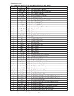
Page 19: ...nput FL GRID output G11 G1 Not connected FL SEGMENT output P35 P32 Power supply input FL SEGMENT output P31 P30 FL SEGMENT output P29 Spectrum analyzer band switching output FL SEGMENT output P28 Spectrum analyzer band switching output Power supply input for FL display FL SEGMENT output P27 Spectrum analyzer band switch output FL SEGMENT output P26 FL SEGMENT output P25 NO CASINO DEMO input to dio...

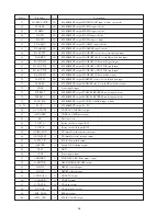
Page 20: ...o diode FL SEGMENT output P16 AM10K input to diode FL SEGMENT output P15 DECK2 cassette detect switch data input FL SEGMENT output P14 DECK2 side B record OK switch data input FL SEGMENT output P13 DECK2 CAM switch signal input FL SEGMENT output P12 DECK1 AUTO STOP signal input FL SEGMENT output P11 DECK2 AUTO STOP signal input FL SEGMENT output P10 DECK1 CAM switch data input FL SEGMENT output P9...

Page 21: ...st L801 so that the voltage between TP3 and TP4 becomes 0V 0 3V Next check that the distortion is less than 1 3 DECK SECTION 10 Tape Speed Adjustment DECK 2 Settings Test tape TTA 100 Test point TP8 Lch TP9 Rch Adjustment location SFR1 Method Play back the test tape and adjust SFR1 so that the frequency counter reads 3000Hz 5Hz and 45Hz REV with respect to forward speed 11 Head Azimuth Adjustment ...

Page 22: ...E EARTH MECH 5 9 12 13 14 15 19 20 21 22 23 24 25 26 27 E H FL401 16 17 18 A A F 36 47 41 37 WIRE BINDER 38 39 A A A A A HT SINK A B C P C B AZG 1 B 40 42 44 I A F G G A A A HT SINK FIN1 A HT SINK FIN2 A 45 46 F A A CHAS MAIN 6ZM 3 43 28 30 31 P C B 33 34 35 H P C B 29 A A ...

Page 23: ...UN 21 8A NFJ 016 010 REFLECTOR FUN 22 8A NFJ 014 010 KEY POWER 23 8A NFJ 015 010 REFLECTOR ECO 24 8A NFJ 019 010 KEY GEQ 25 8A NFJ 029 010 KEY ASSY OPE REV 26 8A NF8 203 010 GUIDE OPE REV 27 8A NF8 201 010 GUIDE FUN 28 88 911 101 110 FF CABLE 11P 1 25 29 88 913 301 110 FF CABLE 13P 1 25 30 8A NFJ 031 010 KEY CD EDIT E A D 30 8A NFJ 025 010 KEY CD EDIT U B C E F 31 8A NFJ 027 010 KEY DISC 32 87 NF4...

Page 24: ...AR CAM M2 33 82 ZM1 227 310 0E LVR TRIG 34 82 ZM3 306 110 0E LVR FR M2 35 82 ZM1 265 110 0E SPR E TRIG 36 87 761 073 410 0E VFT2 2 6 6 W O SLOT 37 82 ZM1 255 310 0E SPR E LVR DIR 38 82 ZM1 322 010 0E SPR T FR60 39 82 ZM1 220 210 0E GEAR IDLER 40 82 ZM3 616 010 0E RING MAGNET 4 41 82 ZM1 216 310 0E GEAR REEL 42 86 ZM3 213 010 0E S SCREW HLDR MOT 3 43 82 ZM1 225 210 0E GEAR FR 44 82 ZM1 226 010 0E G...

Page 25: ... DECK 2 14 12 12 11 5 6 13 3 2 LEVER EJECT R LEVER EJECT L 27 48 53 52 51 57 54 55 56 63 62 49 50 59 HEAD C B D D E F 38 39 40 32 34 33 35 43 45 41 41 44 16 18 47 30 46 8 B CAPSTAN N 2 2 41 7 DECK C B SOL 2 SOL 1 16 D A B C D A 15 A DECK L SIDE DECK R SIDE 36 42 24 C 37 A 58 CAPSTAN N 2 41 5 60 61 E F B E PLATE SHLD M3 C F G H ...

Page 26: ...he PANEL FR 1 Insert the flat head screwdriver tip into the gap between the PANEL FR and the PANEL SPKR Tap the head of the flat head screwdriver with the plastic hammer head and create the clearance as shown in Fig 1 2 Insert the cut chisel in the clearance and tap the head of the cut chisel with plastic hammer as shown in Fig 2 to remove the PANEL FR 3 Place the speaker horizontally Tap head of ...

Page 27: ...2 11 IKENOHATA 1 CHOME TAITO KU TOKYO 110 JAPAN TEL 03 3827 3111 Printed in Singapore 920074 ...

Reviews: