background image

– 23 –

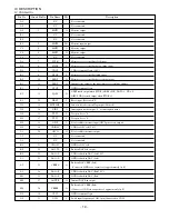
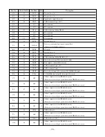
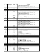
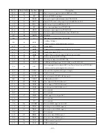
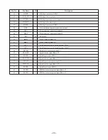
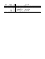
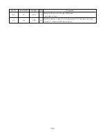
Pin No.

Pin Name

I/O

Description

IC, BD6606KVT

1

SPWIN

I

SPIN detection comparator input (Phase W).

2

SPCOM

I

SPIN motor coil mid-point input terminal.

3

EXTCLK

I

Synchronized clock input terminal.

4 C1P – CHARGEPUMP capacitor 1 conne ct te.

5

C1M

CHARGEPUMP capacitor 1 connect terminal -.

6

C2P

CHARGEPUMP capacitor 2 connect te.

7

C2M

CHARGEPUMP capacitor 2 connect terminal -.

8

VG

O

CHARGEPUMP output.

9

SLVM1

Stepping power part power supply 1.

10

SLUOUT

O

Stepping motor output (Phase U).

11

SLPG1

Stepping power part GND 1.

12

SLVOUT

O

Stepping motor output (Phase V).

13

SLVM2

Stepping power part power supply 2.

14

SLWOUT

O

Stepping motor output (Phase W).

15

SLPG2

Stepping power part GND 2.

16

SLCOM

I

STEP motor coil mid-point input terminal.

17

BEMFW

O

STEP detection comparator output (Phase W).

18

BEMFV

O

STEP detection comparator output (Phase V).

19

BEMFU

O

STEP detection comparator output (Phase U).

20

S3

I

Stepping decoder input 3.

21

S2

I

Stepping decoder input 2.

22

S1

I

Stepping decoder input 1.

23

SGND

Small signal part GND (MOS).

24

ASGND

Small signal part GND (Bip.).

25

STHB

O

H1 and H2 bridge mute terminal.

26

STALL

I

Standby terminal.

27

PW1VM

Half bridge 1 power part power supply.

28

PW1OUT

O

Half bridge 1 output.

29

PWPG

Half bridge power part GND.

30

PW2VOUT

Half bridge 2 output.

31

PW2VM

Half bridge 2 power part power supply.

32

PWIN2

I

Half bridge 2 input.

33

PWIN1

I

Half bridge 1 input.

34

IN2R

I

H bridge 2 reverse input.

35

IN2F

I

H bridge 2 forward input

36

IN1R

I

H bridge 1 reverse input.

37

IN1F

I

H bridge 1 forward input.

38

H2PG2

H bridge 2 power part GND2.

39

H2ROUT

O

H bridge 2 reverse output.

40

H2VM

H bridge 2 power part power supply.

41

H2FOUT

O

H bridge 2 forward output.

42

H2PGI

H bridge 2 power part GND1.
Summary of Contents for AM-HX70

Page 1: ... A T A MINIDISC PLAYER AM HX70 AHK S M Code No 09 009 435 8R1 R E V I S I O N This Service Manual is the Revision Publishing and replaces Simple Manual AM HX70 AHK S M Code No 09 006 435 8T1 BASIC MD MECHANISM AZG F A ...

Page 2: ...sing the supplied rechargeable battery Approx 19 hours with power save on approx 25 hours Using an LR6 size AA dry cell battery Approx 29 hours with power save on approx 38 hours Using the supplied rechargeable battery and an LR6 size AA dry cell battery Approx 51 hours with power save on approx 67 hours Maximum outside Approx 71 6 W X 13 5 H X 77 7 D mm dimensions excluding projected parts and co...

Page 3: ...utsättas för osynling laserstrålning som överskrider gränsen för laserklass 1 PROTECTION OF EYES FROM LASER BEAM DURING SERVICING Precaution to replace Optical block KMS 330A Body or clothes electrostatic potential could ruin laser diode in the optical block Be sure ground body and workbench and use care the clothes do not touch the diode 1 After the connection remove solder shown in right figure ...

Page 4: ... the headphone jack while being careful of the HOLD switch and battery lid 2 Removing the main board 1 Short the short land of the pickup by soldering 2 Remove the three connectors 3 Remove three screws A and screw B 4 While being careful of the FFC of the pickup remove the main board When assembling the parts fasten the screws from screw B and finally remove the short land of the pickup Pickup sh...

Page 5: ...e following procedure 1 Remove the bottom panel and top panel 2 Remove the battery hinge block 3 While bending the boss block of HLDR and CTRG remove HLDR and CTRG in order of 1 and 2 When assembling the parts insert the boss of HLDR and CTRG in order of 2 and 1 4 Remove boss A from the center frame and remove the center frame while lifting up the mechanism in the direction of the arrow 3 HLDR CTR...

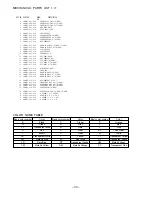
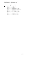
Page 6: ... M P C219 87 A11 049 080 C CAP U 1 6 3 K B C220 87 A11 049 080 C CAP U 1 6 3 K B C301 87 A11 049 080 C CAP U 1 6 3 K B C302 87 A10 561 080 C CAP V 0 01U 16 K B C303 87 A10 561 080 C CAP V 0 01U 16 K B C304 87 A10 561 080 C CAP V 0 01U 16 K B C305 87 A10 770 080 C CAP V 0 1 10 K B C306 87 A10 770 080 C CAP V 0 1 10 K B C308 87 010 787 080 CAP U 0 022 25 C400 87 A10 556 080 C CAP V 2200P 50 K B C401...

Page 7: ... RES V 510K 1 16W F R619 87 A00 762 080 C RES V 680K 1 16W F R701 87 A91 879 080 C F BEAD BK1608TS102 R702 87 A91 879 080 C F BEAD BK1608TS102 DESCRIPTION REF NO KANRI NO PART NO R717 87 A91 878 080 C F BEAD BK1608HS241 R718 87 A91 878 080 C F BEAD BK1608HS241 R719 87 A91 878 080 C F BEAD BK1608HS241 S300 87 A91 436 080 C SW PUSH 2 1 1 SPVE3 8 S301 87 A90 703 080 C SW SL 1 1 3 SSSS813 B 2B S302 87...

Page 8: ... 8 TRANSISTOR ILLUSTRATION B C E 2SA1588 2SA1832 2SC3265 2SC4738 DTA144EE G D S 2SK2009 2SK2035 FDC633N FDC634P D G D S D D ...

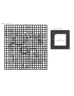
Page 9: ... 91 93 20 88 89 90 21 24 25 85 86 87 22 23 26 82 83 84 29 27 28 78 80 81 30 32 76 77 79 33 34 36 73 74 75 143 147 144 37 46 47 50 53 56 59 64 68 146 72 145 38 40 42 45 48 51 55 57 60 63 66 67 70 39 41 43 44 49 52 54 58 61 62 65 69 71 IC200 CXD2665GA TOP VIEW 31 35 A B C D E F G H J K L M N U P R 1 2 3 4 5 6 7 8 9 10 11 12 13 14 15 16 17 TERMINAL DETAIL FIGURE T 18 19 20 21 22 23 24 25 A B C D E F ...

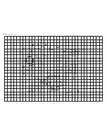
Page 10: ... 10 15 14 13 12 11 10 9 8 7 6 5 4 3 2 1 A B C D E F G H I J K L M N O P Q R S T U 16 17 18 19 20 21 22 23 24 25 26 27 28 29 30 31 32 WIRING 1 MAIN 2 2 ...

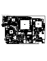
Page 11: ... 11 SCHEMATIC DIAGRAM MAIN FLEX JACK ...

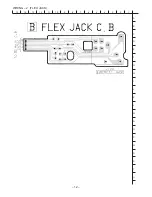
Page 12: ...WIRING 2 FLEX JACK 12 1 2 3 4 5 6 7 8 9 10 11 12 13 14 15 A B C D E F G H I J K L M N O P Q R S T U ...

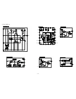
Page 13: ...LOCK DIAGRAM IN 1 MTTC IN 1 VDD VSS VCC INB INA B BSTOUT LPF2 NF2 FB CE EXT GND GND AGCIN OUTB DET OUT EXT FB GND BEEP GND BEEPOA BEEPOB OUTA OUT1 VERFIN VREF LPF1 NF1 IN GND OUT GND MTSW PWSW BSTSW VDD IN VDD ...

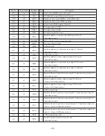
Page 14: ... flag output Not used G 2 16 XINT O Interruption status output L at interruption status G 3 15 TST1 I Test pin Set to L H 1 17 TST2 I Test pin Set to L H 2 19 OSCI I X tal oscillation circuit input OSCI pin reverse output H 3 18 VDIOSC VDD for OSC cell 2 4V J 1 20 OSCO O X tal oscillation circuit output J 2 NC Not connected J 3 NC Not connected K 1 21 VSIOSC GND for OSC cell K 2 24 AOUTL O Built i...

Page 15: ... used U 7 49 A02 O Address output for external DRAM Not used Make sure to leave the pin open when external DRAM is not in use T 7 48 A04 O Address output for external DRAM Not used Make sure to leave the pin open when external DRAM is not in use R 7 47 A03 O Address output for external DRAM Not used Make sure to leave the pin open when external DRAM is not in use U 8 52 A06 O Address output for ex...

Page 16: ...RAM Not used Make sure to leave the pin open when external DRAM is not in use R 13 68 VDC3 VDD for 1 8V internal logic U 14 69 VSC3 VSS for 1 8V internal logic T 14 67 D3 I O Data input output for external DRAM Not used Make sure to leave the pin open when external DRAM is not in use R 14 146 DVDD1 VDD for internal 16Mbit DRAM 2 4V U 17 NC Not connected U 16 NC Not connected U 15 71 XOE O Output e...

Page 17: ...96 TE I Tracking error input from CXA2523AR F 17 99 ADFG I ADIP binary FM signal input 22 05 1kHz from CXA2523AR F 16 98 APC I Error input signal for laser digital APC Auto Power Control from CXS2523AR Connect to analog power supply when not in use F 15 97 DCHG I Connect to low impedance analog power supply E 17 101 VSIO2 VSS for I O cell E 16 102 F0CNT O Control output for CXA2523AR filter cutoff...

Page 18: ...t W Not used Open when not in use C 8 128 SPDV O Brushless spindle motor 3 phase drive logic output V Not used Open when not in use A 7 133 SLDU O Brushless sled motor 3 phase drive logic output U 2 phase drive logic output 1 Open when not in use B 7 132 SPCW I Brushless spindle motor drive comparison input W Not used Connect to GND when not in use C 7 131 SPCV I Brushless spindle motor drive comp...

Page 19: ... I O Description B 4 141 SLVS O Brushless sled motor absolute value PWM output Open when not in use C 4 140 SLCW I O Brushless sled motor 3 phase drive comparison input W Sled 2 phase drive logic output 2 Connect to GND when not in use ...

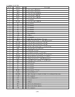
Page 20: ... input L for reduced voltage 21 XINT I Interruption input from CXD2665GA 22 SQSY I SUBQ ADIP synch input 23 KEY I Key input detection input L for key input 24 PSAVE I Power save mode detection SW input L for power save 25 K1HOLD I Main unit HOLD detection SW input L for HOLD 26 PLGI2 I HP plug detection input L during HP plug insertion 27 TEST I Normal TEST mode toggle input L for TEST mode 28 SPF...

Page 21: ...NT O OP power supply control output L for power supply ON 62 OPMUTE O OP mute control output L for mute 63 DRVCNT O BD6606KVT standby output L for standby 64 STHB O Biaxial mute output L for mute 65 NC Not connected 66 NC Not connected 67 NC Not connected 68 NC Not connected 69 NC Not connected 70 NC Not connected 71 SENS I SENS pin signal input from CXD2665GA 72 MNT0 I MNT0 pin signal input from ...

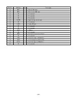
Page 22: ...put 89 NC Not connected 90 AGND Analog GND pin 91 NC Not connected 92 NC Not connected 93 GND GND pin 94 NC Not connected 95 BEEP O Rectangular beep wave detection pin 96 NC Not connected 97 SCLK O Serial clock output to CXD2665GA 98 SRDT I Serial data input from CXD2665GA 99 SWDT O Serial data output to CXD2665GA 100 NC Not connected Pin No Pin Name I O Description ...

Page 23: ...ection comparator output Phase W 18 BEMFV O STEP detection comparator output Phase V 19 BEMFU O STEP detection comparator output Phase U 20 S3 I Stepping decoder input 3 21 S2 I Stepping decoder input 2 22 S1 I Stepping decoder input 1 23 SGND Small signal part GND MOS 24 ASGND Small signal part GND Bip 25 STHB O H1 and H2 bridge mute terminal 26 STALL I Standby terminal 27 PW1VM Half bridge 1 pow...

Page 24: ...l 2 51 FG O FG output 52 BRK I Break comparator input 53 BRK I Break comparator input 54 VCC2 Small signal part power supply terminal 2 Bip 55 VCC1 Small signal part power supply terminal 1 MOS 56 SPVM1 Spindle power part power supply 1 57 SPUOUT O Spindle motor output Phase U 58 SPPG1 Spindle power part GND 1 59 SPVOUT O Spindle motor output Phase V 60 SPVM2 Spindle power part power supply 2 61 S...

Page 25: ...I Standby setting pin H Normal mode L Standby 20 FOCNT I Internal current setting pin 21 VREF O Output reference voltage Not used 22 EQADJ I O EQ central frequency setting pin 23 3TADJ I O BPF3T central frequency setting pin 24 VCC Power supply pin 25 WBLADJ I O BPF22 central frequency setting pin 26 TE O Output tracking error signal 27 CSLED LPF capacitor connection pin for SLED error signal 28 S...

Page 26: ...cuit 44 OPO O Output pin for user operational amplifier Not used 45 OPN I Non inverted input pin for user operational amplifier Connected to GND 46 RFO O RF amplifier output pin Check point for eye pattern 47 MORFI I Input pin where Groove RF signal is AC coupled 48 MORFO O Output pin for Groove RF signal ...

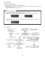
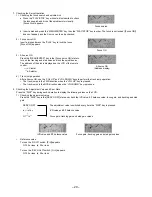
Page 27: ...control works during test mode Test Mode Precautions for handling the disks In the test mode and adjustment mode disks are identified by the HOLD switch on the unit When inserting a disk into the unit check the HOLD switch on the unit Turning on HOLD on the unit Innermost circumference of the MO disk and the PIT disk TEST DISC TGYS 1 etc Turning off HOLD on the unit MO disk groove area MDW 74 disk...

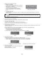
Page 28: ...of 1 kHz 37 2 dB during 10 k output load are output from PHONE OUT 4 Checking Operations of Each Switch The ON OFF state of the switches contact state of the switches on the machine and inside the mechanism can be checked on the LCD of the remote control When all the indicators of the LCD on the remote control light press the STOP key to display SERVO OFF 1 When HOLD on the unit is on the alarm ma...

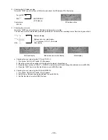
Page 29: ...e the VOL UP and VOL DOWN keys to perform the track jump operation The track jumps in the FWD direction when the VOL UP key is pressed The track jumps in the RVS direction when the VOL DOWN key is pressed 8 Checking the Adjustment Value and Error Rate Press the DISP key during each operation to display the following values on the LCD 1 Checking the adjustment value Press the DISP key in the SERVO ...

Page 30: ... Error rate Jitter Jitter display Address display Address and error rate display Jitter display a Checking the error rate using the PIT disk TGYS 1 1 Turn on the KEY HOLD switch Pi H appears 2 Move the pickup to the position right outside the innermost circumference 3 Press the keys in order of PLAY MODE to set All servo ON and change the address to near 600c 00s 4 Press the DISP key to confirm th...

Page 31: ...d 2 Insert the TGYS 1 and press the PLAY key 3 ADJUST appears on the LCD and the automatic adjustment starts 4 The COMPLETE indication means that the adjustment is completed The SERVO OFF indication means the adjustment is not completed 5 Press the PLAY STOP key then press the DISP key twice Confirm that each of Gf ts is 50 or less 3 Adjustment by the MO disk MDW 74 1 Insert the MDW 74 and press t...

Page 32: ... 32 MECHANICAL EXPLODED VIEW 1 1 AZG F A MAIN C B JACK C B JACK A C A A A B B D C A A 12 1 2 3 4 5 6 7 8 9 10 11 SH PANEL BOT 13 14 16 17 a a a 15 18 19 CUSH BATT ...

Page 33: ...CENTER L L AHK 5 8A HM5 015 010 FRAME CENTER R R AHK 6 8A HM5 216 010 BAT CONTACT 7 8A HM5 007 010 KNOB SL EJECT W AHK L AHK 7 8A HM5 017 010 KNOB SL EJECT R R AHK 8 8A HM3 217 010 SPR E EJECT 9 8A HM5 209 010 PLATE EJECT 10 8A HM5 201 010 FRAME ASSY R 11 8A HM5 006 010 KEY CONT MAIN 12 8A HM3 216 010 BAT CONTACT EX 13 8A HM5 005 010 LID BATT W AHK 13 8A HM5 024 010 LID BATT L L AHK 13 8A HM5 016 ...

Page 34: ...AR A 4 M8 ZZS 294 000 ZZS 2 C 5 8A ZGF 209 010 GEAR B 6 8Z ZG5 217 010 BRG 1 1 2 2 7 8A ZGF 210 010 SHAFT LEAD 8 8A ZGF 212 010 SPR P LEAD 9 87 A91 718 010 PICKUP KMS 330A 10 8Z ZG5 219 010 SPR P RACK 2 A 88 ZG6 224 010 S SCREW VBT 1 4 3 B 8A ZGF 220 010 S SCREW V 1 4 1 2 C 87 067 569 010 POLY WASHER 0 83 2 5 0 25 D 8Z ZG5 223 010 S SCREW VBT 1 4 2 DESCRIPTION REF NO KANRI NO PART NO ...

Page 35: ...30 372 010 HEADPHONE HP M031 L1 L AHK 5 87 B30 295 010 HEADPHONE HP M031 S W AHK R AHK 6 8A HM6 954 010 CLIP RC CL33 7 8A HM3 951 010 BOX BAT ASSY AHM 3 W AHK 7 8A HM5 954 010 BOX BAT ASSY AHM 5 R R AHK 7 8A HM6 952 110 BOX BAT ASSY AHM 6 L L AHK 8 8A HM5 953 010 RC UNIT RC HX70 L L AHK 8 8A HM5 952 010 RC UNIT RC HX70 R R AHK 8 8A HM5 951 010 RC UNIT RC HX70 W W AHK 9 8A HM5 902 010 IB HK ECH ...

Page 36: ...2 11 IKENOHATA 1 CHOME TAITO KU TOKYO 110 JAPAN TEL 03 3827 3111 Printed in Singapore 9301978 0251431 ...

Reviews: