background image

48    PCM-4822 User's Manual

Digital Input and Output Operation

Digital Input and Output are a group of control signals that are
utilized to control external devices requiring ON/OFF circuitry.
The PCM-4822 supports 4-channel digital input and 4-channel
digital output. These digital input and output levels are TTL
compatible.

You can use the I/O read or write command to access the digital
I/O port. An output register has been designed to latch the output
data. However, this cannot be read back for checking purposes.

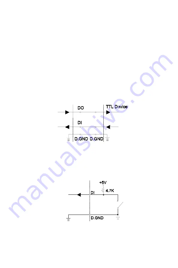
The following figure shows the design of a proposed circuit when
connected with other TTL devices.

When receiving an OPEN/SHORT input signal from a switch or
relay, you are advised to add a pull-up resistor to your system that
will keep the input signal at a high level setting when the circuit is
set to OPEN.

Summary of Contents for PCM-4822

Page 1: ...PCM 4822 486 Based Single Board Computer with Ethernet Interface...

Page 2: ...y infringements upon the rights of third parties which may result from its use Acknowledgements VIA is a trademark of VIA Technology Inc AMD is a trademark of Advanced Micro Devices Inc Award is a tra...

Page 3: ...2 All in One Single Board Computer 1 utility disk with utility programs and Ethernet drivers 1 3 5 IDE flat cable 1 keyboard mouse cable 1 secondary serial port cable RS 232 422 485 1 10 pin pigtail D...

Page 4: ...Safety precautions 13 Installing the CPU 13 Removing a CPU 13 Installing a CPU 14 CPU type select J1 J9 15 CPU power supply select J6 J8 17 CPU clock select J2 J3 J4 17 CMOS setup J14 17 DIO port sele...

Page 5: ...Interface Configuration 27 Chapter 4 Award BIOS Setup 29 System test and initialization 30 System configuration verification 30 AWARD BIOS setup 31 Entering setup 31 Standard CMOS setup 32 BIOS featur...

Page 6: ...2 Expansion bus connector CN6 43 DIO Connector 44 COM2 RS 232 422 485 serial port CN3 44 Keyboard and mouse connector CN8 44 Main power connector J13 45 IDE hard drive connector CN2 45 COM1 RS 232 ser...

Page 7: ...1 General Information This chapter gives background informa tion on the PCM 4822 Sections include Card specifications Card layout and dimensions C H A P T E R...

Page 8: ...o 486DX4 120 CPUs and 5x86 CPUs are supported For maximum performance the PCM 4822 also supports an EDO Normal DRAM SIMM socket that can take up to 32MB memory On board features include support for VL...

Page 9: ...ce Novell NE2000 compatible Built in VL Bus enhanced IDE AT bus hard disk drive interface On board mini DIN PS 2 keyboard mouse connector Two serial ports one RS 232 one RS 232 422 485 selectable uses...

Page 10: ...VL bus devices BIOS auto detect and Mode 3 transfer protocol Serial ports One serial RS 232 port one serial RS 232 422 485 port Two 16550 serial UARTs Keyboard mouse connector Mini DIN connector suppo...

Page 11: ...l Information 5 Mechanical and environmental specifications Dimension WxH 145mmx102mm 5 9 x4 2 Powersupplyvoltage 5V 4 75V 5 25V Max power requirements 5V 2A typical Operatingtemperature 0 60 C 32 140...

Page 12: ...6 PCM 4822 User s Manual Board layout and dimensions PCM 4822 dimensions...

Page 13: ...s chapter tells how to set up the PCM 4822 hardware including instructions on setting jumpers and connecting peripherals switches and indicators Be sure to read all the safety precautions before you b...

Page 14: ...our system to suit your application The table below lists the function of each of the board jumpers and connectors Jumpers Label Function J1 CPU Type Select J2 System clock setting J3 System clock set...

Page 15: ...ctor CN3 Serial port COM2 RS 232 422 485 CN4 Ethernet 10Base T RJ 45 connector CN5 Digital I O connector CN6 Expansion bus connector CN7 Serial port COM1 RS 232 CN8 Keyboard and PS 2 mouse connector L...

Page 16: ...10 PCM 4822 User s Manual Locating jumpers J4 J3 J2 J5 J6 J1 J14 J13 J7 J9 J8 J11 J12 J10...

Page 17: ...r 2 Installation 11 Locating connectors Power LED Y Hard Disk Active G 10Base2 5 AUI CN1 Expansion Bus CN6 Keyboard PS 2 mouse CN8 COM 2 CN3 COM 1 CN7 IDE Hard Disk CN2 Ethernet RJ 45 Connector CN4 DI...

Page 18: ...r you remove the clip Sometimes a jumper will have three pins labeled 1 2 and 3 In this case you would connect either pins 1 and 2 or 2 and 3 The jumper settings are schematically depicted in this man...

Page 19: ...atic dissipative surface or in a static shielded bag when they are not in the chassis Installing the CPU The PCM 4822 all in one SBC supports most 486 CPUs The system s performance depends on the CPU...

Page 20: ...ns and other components 2 Carefully align the CPU so that it is parallel to the socket Make sure that the notch on the corner of the CPU matches the notch on the inside of the socket 3 Gently push the...

Page 21: ...settings for their respective CPUs CPU type select Intel 486DX 25 5V Intel 486DX 33 5V Intel 486DX2 50 Intel 486DX2 66 5V J2 J3 J4 J1 J5 J6 J8 J9 J7 J2 J3 J4 J1 J5 J6 J8 J9 J7 J2 J3 J4 J1 J5 J6 J8 J9...

Page 22: ...5 J6 J8 J9 J7 Default Setting AMD 486DX2 66 3V Cyrix 486DX4 100 AMD 486DX4 100 NV8B Intel 486DX4 100 AMD 486DX4 120 AMD 5x86 P75 TI 486DX2 66 Cyrix 5x86 120 DX5 133 Cyrix 5x86 100GP 3 3V IBM486DX4 100...

Page 23: ...Vcc CPU power supply select 3 3V 3 45V 5V J6 1 3 1 3 3 5 2 4 2 4 4 6 J8 1 2 2 3 CPU clock select J2 J3 J4 J2 J3 and J4 are used to synchronize the CPU clock with the CPU type Set the CPU clock accordi...

Page 24: ...t The procedure for installing SIMMs appears below Please follow these steps carefully 1 Ensure that all power supplies to the system are switched Off 2 Install the SIMM card Install the SIMM so that...

Page 25: ...use a 1 x 44 pin to 2 x 40 pin connector Wire number 1 on the cable is red or blue and the other wires are gray 1 Connect one end of the cable to CN2 Make sure that the red or blue wire corresponds to...

Page 26: ...plications without the system halting under POST power on self test Power connector J13 Main power connector 5V 12V J13 Supplies main power to the PCM 4822 5 V and devices that require 12V Serial port...

Page 27: ...However if you wish to disable the port or change these parameters later you can do this in the system BIOS setup The table below shows the settings for the PCM 4822 board s ports PCM 4822 Serial por...

Page 28: ...22 PCM 4822 User s Manual...

Page 29: ...3 Ethernet Interface Connection This chapter provides information on Ethernet configuration Sections include Network Boot Ethernet Interface Configuration C H A P T E R...

Page 30: ...README DOC NET DIR 1 RSET8019 EXE 2 PG8019 EXE 3 8019AS CFG 4 AWDFLASH EXE 5 4822_SYS BIN ETHERNETDRIVERS 1 RSET8019 EXE This program enables you to view the current Ethernet configura tion reconfigu...

Page 31: ...r AUI CN1 This consists of a 16 pin dual in line male header 10Base T RJ 45 Connector CN4 10Base T connections are made via the on board RJ 45 connector Network Boot The PCM 4822 is shipped with remot...

Page 32: ...ant to save If you wish to continue press Y If you change your mind or have made a mistake press N to abort and end the setup procedure 4 If you decide to continue the screen will issue a prompt which...

Page 33: ...ttings are available PCM 4822 Ethernet Settings IRQ option I O address range Jumperless 2 5 10 200 300EFH Configuration 11 15 Default Settings IRQ 5 Address 300H Note 1 You can select an IRQ from the...

Page 34: ...message guide displayed at the bottom of the screen for additional information 4 After you have made your selections and you are sure that this is the configuration you want press ESC A prompt will ap...

Page 35: ...4 Award BIOS Setup This chapter describes how to set BIOS configuration data C H A P T E R...

Page 36: ...configuration verification These routines check the current system configuration against the values stored in the card s CMOS memory If they don t match the program outputs an error message You will t...

Page 37: ...p information when the power is turned off Entering setup Power on the computer and press Del immediately This will allow you to enter Setup STANDARD CMOS SETUP PASSWORD SETTING BIOS FEATURES SETUP ID...

Page 38: ...ed in the left bottom of the Menu screen CMOS setup screen ROM ISA BIOS 2C4L6AKH STANDARD CMOS SETUP AWARD SOFTWARE INC ESC Quit Select Item PU PD Modify F1 Help Shift F2 Change Color Base Memory 640K...

Page 39: ...nternal Cache Enabled C8000 CBFFF Shadow Disabled Quick Power On Self Test Disabled CC000 CFFFF Shadow Disabled Boot Sequence A C D0000 D3FFF Shadow Disabled Boot Up NumLock Status On D4000 D7FFF Shad...

Page 40: ...S SETUP Esc Quit Select Item F1 Help PU PD Modify F5 Old Values Shift F2 Color F6 Load BIOS Defaults On Board Local Bus IDE Enabled IDEPrimary Master PIO Auto IDE Primary Slave PIO Auto On board Seria...

Page 41: ...OS 2C4L6AKH CMOS SETUP UTILITY POWER MANAGEMENT SETUP Power Management Disabled Doze Mode 8 sec Sleep Timer 2 min Sleep Mode Suspend HDD Power Mngt 1 min VGA Activity Wakeup Disabled IO Activity Disab...

Page 42: ...UP UTILITY AWARD SOFTWARE INC ESC QUIT SELECT ITEM F10 Save Exit Setup Shift F2 Change Color Load BIOS defaults except standard CMOS SETUP Load BIOS defaults LOAD BIOS DEFAULTS loads the default syste...

Page 43: ...ing messages Press Enter 2 If the CMOS is good or this option has been used to change the default password the user is asked for the password stored in the CMOS The screen will display the following m...

Page 44: ...recorded in the chipset s CMOS memory The microprocessor will check this every time you turn your system on and compare this to what it finds as it checks the system This record is required for the sy...

Page 45: ...A The Expansion Bus This appendix provides the basic informa tion on the PCM 4822 expansion bus A P P E N D I X...

Page 46: ...N6 Pin Signal Pin Signal Pin Signal Pin Signal No No No No 1 GND 2 5V 41 GND 42 GND 3 DRQ0 4 DRQ1 43 SMEMRY 44 IOW 5 DRQ2 6 DRQ3 45 MEMCS16 46IDR 7 DRQ5 8 DACK0 47 MEMR 48 IOCS16 9 5V 10 DACK2 49 TC 5...

Page 47: ...or specialized nature It includes 10Base 2 5 AUI connector Ethernet RJ 45 connector Expansion Bus connector DIO connector RS 232 422 485 serial port connector Keyboard and mouse connector Main power c...

Page 48: ...hernet 10Base 2 10Base 5 AUI connector Pin Signal 1 GND 2 CD 3 CD 4 TX 5 TX 6 GND 7 GND 8 RX 9 RX 10 12V 11 GND 12 GND 13 N C 14 N C 15 N C 16 5V Ethernet 10Base T connector CN4 PCM 4822 Ethernet 10Ba...

Page 49: ...12 DACK5 51 SMEMW 52 IOCHRDY 13 DACK3 14 IRQ7 53 REFRESH 54 MEMW 15 IRQ9 16 IRQ10 55 5V 56 GND 17 IRQ11 18 IRQ15 57 GND 58 N C 19 LA23 20 LA22 59 BALE 60 SBHE 21 LA21 22 LA20 61 LA19 62 LA18 23 IRQ5...

Page 50: ...r Pin Signal 1 GND 2 Vcc 3 DO3 4 DO2 5 DO1 6 DO0 7 DI3 8 DI2 9 DI1 10 DI0 COM2 RS 232 422 485 serial port CN3 PCM 4822 COM2 RS 232 422 485 serial port Pin Signal 1 DCD 2 DSR 3 RxD 4 RTS 5 TxD 6 CTS 7...

Page 51: ...ctor J13 PCM 4822 Main power connector Pin Signal 1 12 V 2 GND 3 GND 4 5 V IDE hard drive connector CN2 PCM 4822 IDE hard drive connector Pin Signal Pin Signal 1 IDE RESET 2 GND 3 DATA 7 4 DATA 8 5 DA...

Page 52: ...IO CHANNEL READY 28 N C 29 N C 30 GND 31 IRQ14 32 IOCS16 33 ADDR 1 34 N C 35 ADDR 0 36 ADDR 2 37 HARD DISK SELECT 0 38 HARD DISK SELECT 1 39 IDE ACTIVE 40 MGND 41 VCC 42 MVCC 43 GND 44 N C COM1 RS 23...

Page 53: ...Digital Input and Output Operations This appendix contains some basic information on the Digital Input and Output operation of the PCM 4822 board Digital input and output operation Digital I O Interf...

Page 54: ...compatible You can use the I O read or write command to access the digital I O port An output register has been designed to latch the output data However this cannot be read back for checking purpose...

Page 55: ...Low 0 8V max Input Load High 0 05mA max at 2 7V Low 0 4mA max at 0 5V Register Address 340H or 240H Read Register Format BIT D3 D2 D1 D0 Value DI3 DI2 DI1 DI0 Digital Output Output channels 4 bits Le...

Page 56: ...50 PCM 4822 User s Manual...

Reviews: