background image

PCIE-1840 User Manual

8

2.1

Unpacking

After receiving your PCIE-1840 package, inspect its contents first.

The package should contain the following items:

PCIE-1840 card

Auto-Calibration Board

Companion CD-ROM (DLL driver included)

Startup Manual

The PCIE-1840 cards harbors certain electronic components vulnerable to electro-
static discharge (ESD). ESD could easily damage the integrated circuits and certain
components if preventive measures are not carefully paid attention to.

Before removing the card from the antistatic plastic bag, you should take following
precautions to prevent ESD damage:

Touch a metal part of your computer chassis with your hand to discharge static 
electricity accumulated on your body. Or use a grounding strap.

Touch the anti-static bag to a metal part of your computer chassis before open-
ing the bag.

Hold the card only by the metal bracket when removing it from the bag.

After taking out the card, you should first inspect the card for any possible signs of
external damage (loose or damaged components, etc.). If the card is visibly dam-
aged, please notify our service department or the local sales representative immedi-
ately. Avoid installing a damaged card into your system. Also, pay extra caution to the
following aspects to ensure proper installation:

Avoid physical contact with materials that could hold static electricity such as 
plastic, vinyl and Styrofoam.

Whenever you handle the card, grasp it only by its edges. DO NOT TOUCH the 
exposed metal pins of the connector or the electronic components.

2.2

Driver Installation

We recommend you install the driver before you install the PCIE-1840 card into your
system, since this will guarantee a smooth installation process.

The Advantech DAQNavi Device Drivers Setup program for the PCIE-1840 card is
included in the companion DVD-ROM that is shipped with your DA&C card package.
Please follow the steps below to install the driver software:

1.

Insert the companion DVD-ROM into your DVD-ROM drive.

2.

The Setup program will be launched automatically if you have the auto play 
function enabled on your system. When the Setup Program is launched, you 
can follow the installation guide to correctly install the driver step by step.

Note!

Keep the anti-static bag for future use. You may need the original bag to 
store the card if you have to remove the card from the PC or transport it 
elsewhere.

Summary of Contents for PCIE-1840

Page 1: ...User Manual PCIE 1840 4 ch 16Bit 125 MS s High Speed Data Acquisition PCI Express Card ...

Page 2: ...ion Advantech assumes no liability under the terms of this warranty as a consequence of such events Because of Advantech s high quality control standards and rigorous testing most of our customers never need to use our repair service If an Advantech product is defec tive it will be repaired or replaced at no charge during the warranty period For out of warranty repairs you will be billed according...

Page 3: ...chments Description of your software operating system version application software etc A complete description of the problem The exact wording of any error messages Packing List Before setting up the system check that the items listed below are included and in good condition If any item does not accord with the table please contact your dealer immediately PCIE 1840 DA C card Startup or User Manual...

Page 4: ...PCIE 1840 User Manual iv ...

Page 5: ...uration 9 Figure 2 1 The Device Setting of PCIE 1840 9 Figure 2 2 The Device Setting page 10 Figure 2 3 The Device Testing of PCIE 1840 11 Chapter 3 Signal Connections 13 3 1 Overview 14 3 2 Jumper Settings 14 Table 3 1 Board ID Settings 14 3 3 Signal Connections 15 Figure 3 1 19 pin I O Connector Pin Assignments 15 3 3 1 I O Connector Signal Description 15 3 3 2 Trigger Type 16 Figure 3 2 Digital...

Page 6: ...uit 26 Figure A 2 Phase response of AC coupling circuit 26 A 6 AI Input Bandwidth and Settling 27 A 6 1 Tunable Capacitor for One tenth Voltage Divider in 1Mohm 27 Figure A 3 PCIE 1840 one tenth divider Circuit 27 Figure A 4 Without capacitors compensation the settling time is quite slow 28 Figure A 5 With compensation settling time is much faster 28 Appendix B Block Diagram 29 B 1 Overview 30 Fig...

Page 7: ... tion on the features of the PCIE 1840 cards a quick installation guide together with some brief information on software and accessories Sections include Features Applications Installation Guide Software Overview Device Drivers Programming Roadmap Accessories ...

Page 8: ... 1840 card features software auto calibration It provides a convenient method for user calibration processing 1 2 2 BoardID Switch The PCIE 1840 has a built in DIP switch that helps define each card s ID when multi ple PCIE 1840 cards have been installed on the same PC chassis The BoardID set ting function is very useful when building a system with multiple PCIE 1840 cards With the correct BoardID...

Page 9: ...ws8 desktop mode 7 and XP Some optional components are also available for enhanced operation After you get the necessary components and maybe some of the accessories for enhanced opera tion of your Multifunction card you can then begin the installation procedures Figure 1 1 on the next page provides a concise flow chart for a broad picture of the software and hardware installation procedure Figure...

Page 10: ...ng Tools Programmers can develop application programs with their favorite development tools Visual Studio Net Visual C and Visual Basic Delphi C Builder For instructions on how to begin programming works in each development tool Advantech offers a Tutorial Chapter in the DAQNavi SDK Manual for your reference Refer to the corresponding sections in this chapter on the DAQNavi SDK Manual to begin you...

Page 11: ... Event Function Group For the usage and parameters of each function please refer to the Using DAQNavi SDK chapter in the DAQNavi SDK Manual 1 6 3 Troubleshooting Device Drivers Error Driver functions will return a status code when they are called to perform a certain task for the application When a function returns a code that is not zero it means the function has failed to perform its designated ...

Page 12: ...PCIE 1840 User Manual 6 ...

Page 13: ...Chapter 2 2 Installation ...

Page 14: ...ur service department or the local sales representative immedi ately Avoid installing a damaged card into your system Also pay extra caution to the following aspects to ensure proper installation Avoid physical contact with materials that could hold static electricity such as plastic vinyl and Styrofoam Whenever you handle the card grasp it only by its edges DO NOT TOUCH the exposed metal pins of ...

Page 15: ...ace Use of excessive force must be avoided otherwise the card might be damaged 6 Fasten the bracket of the PCI card on the back panel rail of the computer with screws 7 Plug in the power cord and turn on the computer 2 3 Device Setup Configuration The Advantech Navigator program is a utility that allows you to set up configure and test your device and later stores your settings on the system regis...

Page 16: ...ser Manual 10 Configuring the Device Go to the Device Setting to configure your device Here you can configure not only the Analog Input of PCIE 1840 but also Digital Input Output Figure 2 2 The Device Setting page ...

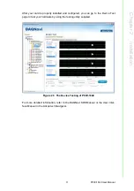
Page 17: ...stalled and configured you can go to the Device Test page to test your hardware by using the testing utility supplied Figure 2 3 The Device Testing of PCIE 1840 For more detailed information refer to the DAQNavi SDK Manual or the User Inter face Manual in the Advantech Navigator ...

Page 18: ...PCIE 1840 User Manual 12 ...

Page 19: ...tions This chapter provides useful information about how to connect input and output signals to the PCIE 1840 cards via the I O con nector Sections include Overview Switch Settings Signal Connections Field Wiring Considerations ...

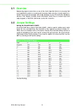
Page 20: ... to define each card s board ID You can determine the board ID on the register as shown in Table 3 1 When there are multiple cards on the same chassis this board ID setting function is useful for identifying each card s device number through board ID We set the PCIE 1840 board ID as 0 at the factory If you need to adjust it to other board ID set the SW1 by referring to DIP switch setting Default S...

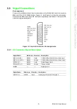
Page 21: ...e 3 1 shows its I O connector signal description Figure 3 1 19 pin I O Connector Pin Assignments 3 3 1 I O Connector Signal Description Signal Name Reference Direction Description REF_CLK_IN DGND Input 10 MHz differential reference clock input REF_CLK_OUT DGND Output 10 MHz differential reference clock output DTRG 0 1 DGND Input Digital trigger inputs TRIGOUT 0 1 DGND Output Trigger outputs DGND D...

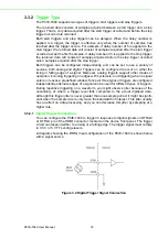
Page 22: ...ising or falling edge of a signal Moreover analog triggers support other modes of operation including triggering on edges with hysteresis and triggering when a signal enters or leaves a predefined window Since all three types of triggers are configured independently alternate edges of a signal can be used for different types of triggers During repetitive triggering on a waveform you might observe ...

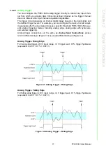
Page 23: ...s after the input signal crosses a specific threshold PCIE 1840 offers sev eral analog triggering modes including analog edge analog edge with hysteresis and window triggering Analog trigger connections are the same as Analog Input Connections please refer to differential input Figure 3 3 or pseudo differential input Figure 3 4 Analog Trigger Rising Edge For rising edge trigger 10 V input range 2 ...

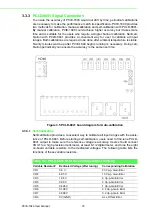
Page 24: ...nsure the accuracy is the same over time Figure 3 5 PCLD 8841 board diagram for Auto calibration 3 3 3 1 Self Calibration Self calibration provides a convenient way to calibrate all input ranges with the assis tance of PCLD 8841 Before starting self calibration users need to fine tune PCLD 8841 output to make sure the reference voltage is accuracy Users should connect VOUT to a high precision mult...

Page 25: ...cquisition system If the cable travels through an area with significant electromagnetic interference you should adopt individually shielded twisted pair wires as the analog input cable This type of cable has its signal wires twisted together and shielded with a metal mesh The metal mesh should only be connected to one point at the sig nal source ground Avoid running the signal cables through any c...

Page 26: ...PCIE 1840 User Manual 20 ...

Page 27: ...Appendix A A Specifications ...

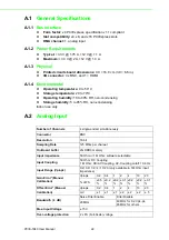
Page 28: ...RH non condensing Indoor use only A 2 Analog Input Number of Channels 4 single ended simultaneously Connector BNC Resolution 16 bit Sampling Rate 125 MS s per channel On Board buffer 2G DDR3 memory Input impedance 50 Ohm or 1M Ohm software selectable Input Coupling 50 Ohm DC Coupling 1 M Ohm DC AC Coupling AC Coupling cutoff 10 6 Hz Input Range Vpk pk 0 2 0 4 1 2 4 10 20 only available in 1M Ohm i...

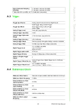
Page 29: ...ling software selectable Analog Trigger Filter 50 KHz Low Pass filter software selectable Digital Trigger Level 3 3 V COMS compatible Low 0 8 V max High 2 0V min Digital Trigger pulse width 50 ns min Digital Trigger Polarity Rising or Falling edge software selectable Number of Digital Trigger Output 2 Digital Trigger Output Source Analog Trigger Input Digital Trigger input or Software Trigger Digi...

Page 30: ... 61 5 1 0 V 71 5 64 5 71 64 0 5 V 70 63 5 69 5 63 0 2 V 66 61 64 60 5 0 1 V 61 58 5 58 5 57 100 kHz input tone input amplitude is 1 dBFS Signal to Interference and Noise Ratio dB Input Impedance 50 Input Impedance 1M Input Range Filter ON Filter OFF Filter ON Filter OFF 10 0 V N A N A 69 64 5 0 V 71 64 68 5 63 5 2 0 V 67 61 5 65 61 5 1 0 V 71 5 64 71 64 0 5 V 69 5 63 5 69 63 0 2 V 65 5 61 64 60 0 ...

Page 31: ... 0 V 67 61 5 65 61 5 1 0 V 71 5 64 71 64 0 5 V 69 5 63 5 69 63 0 2 V 65 5 61 64 60 0 1 V 61 58 5 58 5 57 100 kHz input tone input amplitude is 1 dBFS Spurious Free Dynamic Range dB Input Impedance 50 Input Impedance 1M Input Range Filter ON Filter OFF Filter ON Filter OFF 10 0 V N A N A 72 75 5 0 V 87 87 74 5 76 2 0 V 86 5 82 78 84 1 0 V 85 83 86 84 5 0 5 V 85 84 86 85 5 0 2 V 84 5 85 78 79 5 0 1 ...

Page 32: ...PCIE 1840 User Manual 26 A 5 8 AC Coupling 3 dB cutoff frequency 10 6 HZ 1M Ohm input impedance only Figure A 1 Magnitude response of AC coupling circuit Figure A 2 Phase response of AC coupling circuit ...

Page 33: ...input impedance With large 1M Ohm input impedance any small parasitic capacitance could seriously affect the input impedance To compensate the loss tunable capaci tors are added along the one tenth divider Users can get the better performance by fine tuning the tunable capacitor Here are the figures to describe the issue Trim Capacitor Function 1M input impedance only TC400 Analog input channel 0 ...

Page 34: ...tion the settling time is quite slow Figure A 5 With compensation settling time is much faster For the users requiring high frequency applications it s highly recommended to select 50 Ohm input impedance to ease the known overshoot and parasitic capaci tance issue ...

Page 35: ...Appendix B B Block Diagram ...

Page 36: ...PCIE 1840 User Manual 30 B 1 Overview Figure B 1 Function block diagram overview B 2 Analog Input TIS Function Figure B 2 Dual ADCs combination architecture in TIS mode ...

Page 37: ...m each ADC are interleaved to construct a waveform as like a single ADC dose The following figures describe how TIS works The mismatches between multiple ADCs will degrade the performance of PCIE 1840 They will lead to voltage swings in time domain and unexpected spurs in fre quency domain These mismatches include offset mismatch gain mismatch and clock phase mismatch Though PCIE 1840 is capable t...

Page 38: ...ations are subject to change without notice No part of this publication may be reproduced in any form or by any means electronic photocopying recording or otherwise without prior written permis sion of the publisher All brand and product names are trademarks or registered trademarks of their respective companies Advantech Co Ltd 2015 ...

Reviews: