background image

PCA-6763 User Manual

48

3.2.3.3.4

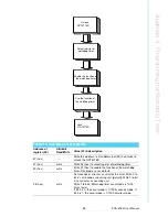
Restore on AC Power Loss

This item allows you to select system restore states if AC power loss.

3.2.3.3.5

Wake On Ring

Enable or disable wake on ring.

3.2.3.3.6

Port 80h Redirection 

Control where the port 80h cycles are sent.

3.2.4

Boot Configuration

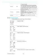
Setup Prompt Timeout

This item allows you to change number of seconds to wait for setup activation
key.

Bootup NumLock State

Select the Power-on state for Numlock. 

Quiet Boot

If this option is set to Disabled, the BIOS displays normal POST messages. If
Enabled, an OEM Logo is shown instead of POST messages. 

GateA20 Active

This item allows you to select Upon request or Always.

Option ROM Messages

Set display mode for option ROM. 

Interrupt 19 Capture 

This item allows option ROMs to trap interrupt 19.

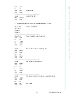
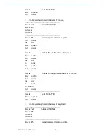
Boot Option 

Sets the system boot order.

Summary of Contents for PCA-6763

Page 1: ...orldwide with offices in Germany Austria Switzerland Great Britain and the USA For more information please contact FORTEC Elektronik AG Hauptniederlassung Lechwiesenstr 9 86899 Landsberg am Lech Telefon 49 0 8191 91172 0 Telefax 49 0 8191 21770 E Mail sales fortecag de Internet www fortecag de FORTEC Elektronik AG Büro West Hohenstaufenring 55 50674 Köln Telefon 49 0 221 272 273 0 Telefax 49 0 221...

Page 2: ...User Manual PCA 6763 AMD T16R ISA Half size SBC with Dual Independent Display Dual GbE SATA USB m SATA COM LPT ...

Page 3: ...ch assumes no liability under the terms of this warranty as a consequence of such events Because of Advantech s high quality control standards and rigorous testing most of our customers never need to use our repair service If an Advantech product is defec tive it will be repaired or replaced at no charge during the warranty period For out of warranty repairs you will be billed according to the cos...

Page 4: ... concern Here is a guide to Advantech s customer services To ensure you get the full benefit of our services please follow the instruc tions below carefully Technical Support We want you to get the maximum performance from your products So if you run into technical difficulties we are here to help For the most frequently asked questions you can easily find answers in your product documentation The...

Page 5: ...dor PN Memory Advantech PN Transcend 1GB DDR3 1066 SODIMM DDR3 N TS128MSK64V1U SEC K4B1G0846G BCH9 96SD3 1G1066NN TR Transcend 2GB DDR3 1066 SODIMM DDR3 N TS128MSK64V1U SEC HCH9 K4B1G0846D 128x8 96SD3 2G1066NN TR Transcend 4GB DDR3 1066 SODIMM DDR3 N TS7KSN28420 1Y HYNIX H5TQ2G83BFR 256x8 96SD3 4G1066NN TR Warning Due to limited compatibility of onboard memory Strongly suggest to choose above memo...

Page 6: ...fications notify our service department or your local sales representative immediately Also notify the carrier Retain the shipping carton and packing material for inspection by the carrier After inspection we will make arrangements to repair or replace the unit 1 PCA 6763 PICMG 1 0 Half size single board computer 1 PCA 6763 startup manual P N 2006A67600 1 CD with utility P N 2066A67600 1 Serial AT...

Page 7: ...PCA 6763 User Manual vi ...

Page 8: ...Selection ATXF1 8 1 8 4 LVDS Backlight setting JVBR1 and LVDS panel voltage selection JLVDS1 9 Table 1 5 LVDS Backlight Setting VBR1 9 Table 1 6 LVDS panel voltage selection JLVDS1 9 1 8 5 Hardware monitor alarm JOBS1 and Watchdog timer output JWDT1 10 Table 1 7 H W monitor alarm and Watchdog timer JOBS1 JWDT1 10 1 9 Keyboard Lock and Buzzer Setting 10 Table 1 8 Keyboard lock KL1 10 Table 1 9 Buzz...

Page 9: ... 3 2 Main setup screen 29 3 2 2 Advanced BIOS Features Setup 30 3 2 3 Chipset Configuration 43 3 2 4 Boot Configuration 48 3 2 5 Security Configuration 49 3 2 6 Save Exit 50 Chapter 4 Value Added Software Services 51 4 1 Value Added Software Services 52 4 1 1 Software API 52 Chapter 5 Chipset Software Installation Utility 53 5 1 Before You Begin 54 5 2 Windows XP Windows 7 Driver Setup 54 Chapter ...

Page 10: ...D1 70 Table B 9 Hi definition audio link connector HDAUD1 70 B 9 LAN1 and LAN2 LED Connector LANLED1 71 Table B 10 LAN1 and LAN2 LED connector LANLED1 71 B 10 GPIO Header GPIO1 71 Table B 11 GPIO header GPIO1 71 B 11 JIR1 72 Table B 12 JIR1 72 B 12 JCASE1 72 Table B 13 JCASE1 72 B 13 LPC1 73 Table B 14 LPC1 73 B 14 PWR1 73 Table B 15 PWR1 73 B 15 DVI1 74 Table B 16 DVI1 74 B 16 LVDS1 75 B 17 Syste...

Page 11: ...PCA 6763 User Manual x ...

Page 12: ...Chapter 1 1 Hardware Configuration ...

Page 13: ...erfaces Users can purchase Advantech COM mod ule P N PCA COM485 00A1E and PCA COM232 00A1E to have four extra serial ports with auto flow control capability In addition to board level products Advantech also offers a series of small form fac tor wall mount chassis With the low power compact sized high reliability and sys tem level solutions PCA 6763 is the ideal computing platform for modern indus...

Page 14: ... Two RS 232 serial ports on board Extra four RS 232 or RS 422 485 serial ports supported by optional COM module via low pin count connector P N PCA COM232 00A1E PCA COM485 00A1E PS 2 keyboard and mouse connector 1 6 pin DIN socket on bracket for PS 2 keyboard and mouse USB port G2 SKU USB 2 0 x7 1 on bracket 6 onboard VG SKU USB 2 0 x6 6 on board SATA Four SATA 3 0 ports 600 MB s m SATA One m SATA...

Page 15: ...KU Supporting dual 10 100 1000 Mbps Ethernet ports with Realtek RTL8111E VL CG VG SKU Supporting single 10 100 1000 Mbps Ethernet port with Realtek RTL8111E VL CG 1 3 6 Industrial features Watchdog timer Can generate a system reset or IRQ11 The watchdog timer is programmable with each unit equal to one second or one minute 255 lev els 1 3 7 Mechanical and environmental specifications Operating tem...

Page 16: ... ATX mode selection JVBR1 LVDS backlight setting JLVDS1 LVDS panel voltage selection Table 1 2 Connectors Label Function LPT1 Parallel port supports SPP EPP ECP mode LAN1 Realtek RTL8111E VL CG LAN2 G2 SKU only Realtek RTL8111E VL CG VGA1 VGA connector KBMS1 External keyboard mouse connector KBMS2 Internal keyboard mouse connector COM12 Box header for RS 232 2 JIR1 Infrared connector JFP1 Power Sw...

Page 17: ...onnector Locations Figure 1 1 Jumper and connector locations JFP1 BZ1 SMBUS1 USB12 USB34 GPIO1 SATA4 SATA3 SATA2 SATA1 LPT1 FDD1 JIR JOBS1 JWDT1 COM12 USB56 USB7 LAN2 LAN1 VGA1 KBMS1 PWR1 ATXF1 DVI1 LVDS1 KL1 JVBR1 LANLED1 PC 104 HDAUD1 JCASE1 KBMS2 INV1 ...

Page 18: ... electronics personnel should open the PC chassis Caution Always ground yourself to remove any static charge before touching the motherboard Modern electronic devices are very sensitive to static electrical discharges As a safety precaution use a grounding wrist strap at all times Place all electronic components on a static dissipative surface or in a static shielded bag when they are not in the c...

Page 19: ... information Normally this jumper should be set with pins 1 2 closed If you want to reset those data set JCMOS1 to 2 3 closed for just a few sec onds and then move the jumper back to 1 2 closed This procedure will reset the CMOS to its last status or default setting Please note that both date and time information will be reset after short pin 2 3 1 8 3 AT ATX mode HW selection ATXF1 The PCA 6763 c...

Page 20: ...panel offers jumper to set backlight mode and panel voltage Table 1 5 LVDS Backlight Setting VBR1 Function Jumper Setting Linear way to control brightness PWM to control brightness Default setting Table 1 6 LVDS panel voltage selection JLVDS1 Function Jumper Setting 3 3V 1 3 closed 5V 3 5 closed 12V 3 4 closed Default setting 1 2 closed 1 2 3 2 3 closed 1 2 3 ...

Page 21: ... also provide jumper JOBS1 to enable or disable hardware monitor func tion 1 9 Keyboard Lock and Buzzer Setting PCA 6763 provides jumpers for customer to enable keyboard lock and buzzer via hardware settings Table 1 7 H W monitor alarm and Watchdog timer JOBS1 JWDT1 Function Jumper Setting Enable watchdog timer Enable H W monitor alarm default setting Table 1 8 Keyboard lock KL1 Function Jumper Se...

Page 22: ...Chapter 2 2 Connecting Peripherals ...

Page 23: ...If you have a num ber of cards installed you may need to partially remove a card to make all the con nections 2 2 Parallel Port LPT1 The parallel port is normally used to connect the motherboard to a printer PCA 6763 includes an onboard parallel port accessed through a 26 pin flat cable connector LPT1 LPT1 ...

Page 24: ...Specification 2 0 support transfer rates up to 480 Mbps USB 1 6 ports are located on board with box header and USB7 G2 is on rear I O bracket The USB interface can be disabled in the system BIOS setup 2 4 VGA Connector VGA1 This CPU card has VGA outputs that can drive conventional CRT displays VGA1 is a standard 15 pin D SUB connector commonly used for VGA AMD driver can help for both VGA extended...

Page 25: ... 1700008822 for standard DVI connector on bracket 2 6 LVDS LVDS1 For G2 SKU LVDS1 for dual channel 24 bit LVDS panel and for VG SKU LVDS1 is for 18 bit panel Please check the pin define before installing your panel DVI1 LVDS1 1 3 5 7 9 11 13 15 17 19 21 23 25 27 29 31 33 35 37 39 2 4 6 8 10 12 14 16 18 20 22 24 26 28 30 32 34 36 38 40 ...

Page 26: ...n Signal 1 V_LCD 21 LVDS0_D2 2 V_LCD 22 LVDS1_D2 3 GND 23 GND 4 GND 24 GND 5 V_LCD 25 LVDS0_CLK 6 V_LCD 26 LVDS1_CLK 7 LVDS0_D0 27 LVDS0_CLK 8 LVDS1_D0 28 LVDS1_CLK 9 LVDS0_D0 29 GND 10 LVDS1_D0 30 GND 11 GND 31 LVDS0_DDC_CLK 12 GND 32 LVDS0_DDC_DAT 13 LVDS0_D1 33 GND 14 LVDS1_D1 34 GND 15 LVDS0_D1 35 LVDS0_D3 16 LVDS1_D1 36 LVDS1_D3 17 GND 37 LVDS0_D3 18 GND 38 LVDS1_D3 19 LVDS0_D2 39 LVDS0_ENABK...

Page 27: ... printer or to a communications network The IRQ and address ranges for both ports are fixed However if you want to disable the port or change these parameters later you can do this in the system BIOS setup 2 9 PS 2 Keyboard and Mouse Connector KBMS1 Two on board 6 pin mini DIN connectors KBMS1 provide connection to PS 2 key board COM12 KBMS1 ...

Page 28: ...ont Panel Connectors JFP1 FP1 is a 10 pin connector which connects to the front panel switch to control system power on off and reset Table 2 1 Power LED status Power mode LED System On On System Suspend Fast flashes System Off Off System Off in deep sleep Off JFP1 ...

Page 29: ... 10 Closed Enables hardware monitor alarm Default 8 10 Open Disables hardware monitor alarm 2 11 2 Watchdog timer JWDT1 This is for an setting action trigger on the watchdog timer 4 6 Close Enable watchdog timer Default 4 6 Open No action 2 11 3 Infrared interface JIR1 This is a 5 pin header for an infrared device JIR1 JOBS1 JWDT1 1 3 5 7 9 2 4 6 8 10 JWDT1 JOBS1 JIR1 ...

Page 30: ...r network operating systems The RJ 45 jacks on the rear plate provide convenient connectivity Table 2 2 LAN LED Indicators LAN Mode LED1 LED2 1000Mbps Link On Green On On 1000Mbps Active Green on Flash 1000Mbps Link Off Off Off 100Mbps Link On Orange On On 100Mbps Active Orange On Flash 100Mbps Link Off Off Off 10Mbps Link On Off On 10Mbps Active Off Flash 10Mbps Link Off Off Off LAN2 LAN1 ...

Page 31: ...on Audio Module Interface HDAUD1 This HDAUD1 pin header is the connection interface to Advantech s 7 1 channel high definition audio module Note Advantech 7 1 channel high definition audio module ordering informa tion P N PCA AUDIO HDA1E HDAUD1 ...

Page 32: ...cations of PCA AUDIO HDA1E Connect CN1 with the power supply s 4 pin power connector Connect HDAUD1 to the HDAUD1 pinheader on the CPU card with the HD audio cable PN 1701120251 Connect CDIN1 with the CD DVD drive s CD in connector with the audio line included i in the CD DVD drive accessory ...

Page 33: ... Digital I O usage Refer to Appendix B for detailed information on the pin assignments and programming guide in Appendix C 2 15 Case Open Connector JCASE1 The 2 pin case open connector is for chassis with a case open sensor When the case is open the buzzer on motherboard will beep GPIO1 JCASE1 ...

Page 34: ...Panel LAN Indicator Connector LANLED1 Table 2 3 LAN LED Indicators LAN Mode LED 1000Mbps Link On On 1000Mbps Active Flash 1000Mbps Link Off Off 100Mbps Link On On 100Mbps Active Flash 100Mbps Link Off Off 10Mbps Link On On 10Mbps Active Flash 10Mbps Link Off Off LANLED1 ...

Page 35: ...mance serial ATA interface 600MB s which eases cabling to hard drivers or CD DVD drivers with long cables 2 18 LPC Extension Interface LPC1 LPC1 is a 14 pin female pinheader for adopting Advantech LPC module such as PCA COM232 00A1E PCA COM485 00A1E PCA TPM 00A1E SATA4 SATA3 SATA2 SATA1 LPC1 ...

Page 36: ...er Manual Chapter 2 Connecting Peripherals 2 19 12 5v power connector PWR1 2 20 PC 104 PCA 6763 provide PC 104 connector for customer s module applications PWR1 Note UEFI code do not support PC 104 VGA module PC 104 ...

Page 37: ...PCA 6763 User Manual 26 ...

Page 38: ...Chapter 3 3 AMI BIOS Setup ...

Page 39: ...modify BIOS settings and control the special features of your computer The Setup program uses a number of menus for making changes and turning the special features on or off This chapter describes the basic navigation of PCA 6763 setup screens Figure 3 1 Setup program initial screen ...

Page 40: ...ame displays all the options that can be configured Grayed out options cannot be configured options in blue can The right frame displays the key legend Above the key legend is an area reserved for a text message When an option is selected in the left frame it is highlighted in white Often a text message will accom pany it System Time System Date Use this option to change the system time and date H...

Page 41: ...by highlighting it using the Arrow keys All Advanced BIOS Setup options are described in this section The Advanced BIOS Setup screens is shown below The sub menus are described on the following pages 3 2 2 1 Legacy OpROM support Launch PXE OpROM Enable or disable boot options for legacy network devices The item works simultaneously on LAN1 and LAN2 Launch Storage OpROM Enable or disable boot optio...

Page 42: ... PCI Latency Timer This item allows you to select the 32 64 96 128 160 192 224 248 PCI bus clocks VGA Palette Snoop Enabled or disable VGA palette registers snooping PERR Generation Enabled or disable PCI device to generation PERR SERR Generation Enabled or disable PCI device to generation SERR ...

Page 43: ...6763 User Manual 32 3 2 2 3 ACPI Settings Configuration Power Type Choosing this item correspond with your power supply type AT or ATX Enable Hibernation Enable or disable hibernation function if OS support ...

Page 44: ...apter 3 AMI BIOS Setup 3 2 2 4 S5 RTC Wake Settings Wake system with Fixed Time Enable or disable system wake on alarm event by user define 3 2 2 5 Trusted Computing TPM Support Enable or disable BIOS support for security device ...

Page 45: ...PC Adjustment This item allows you to provide _PPC object NX Mode This item allows you to enable or disable the No execute page protection func tion SVM Mode This item allows you to enable or disable the CPU virtualization C6 Mode This item allows you to auto or disable C6 function CPB Mode This item allows you to auto or disable CPB Node 0 Information View detail of memory information related to ...

Page 46: ...35 PCA 6763 User Manual Chapter 3 AMI BIOS Setup 3 2 2 7 IDE Configuration ...

Page 47: ...f This is a workaround for OSes without EHCI hand off support The EHCI owner ship change should claim by EHCI driver USB transfer time out Time out value for control Bulk and interrupt transfers Device reset time out USB mass storage device start unit command time out Device power up delay Maximum time the device will take before it properly report itself to the host con troller ...

Page 48: ...apter 3 AMI BIOS Setup 3 2 2 9 Super I O Configuration 3 2 2 9 1Floppy Disk Controller Configuration Floppy Disk Controller Enable or disable floppy disk controller Change Settings Select an optimal setting for super I O device ...

Page 49: ... Mode Change mode of floppy disk controller Select read write for normal operation Select write protect mode for read only operation 3 2 2 9 2Serial Port1 and Serial Port2 Configuration Serial Port Enable or disable serial port COM ...

Page 50: ...n optimal setting for super I O device Device mode Change the serial port mode 3 2 2 9 3Parallel Port Configuration Parallel Port Enable or disable parallel port LPT LPTE Change Settings Select an optimal setting for super I O device Device Mode Change the printer port mode ...

Page 51: ...A 6763 User Manual 40 3 2 2 10 H W Monitor Case Open Warning Enable or disable case open warning CPU Warning Temperature Set CPU warning temperature ACPI Shutdown Temperature Set ACPI shutdown temperature ...

Page 52: ...BIOS Setup 3 2 2 11 IT8888 Configuration ITE8888 ISA Decode Section for ISA positively decode or subtractive decode Memory Hole 15MB 16MB Enable or disable memory hole 15 16MB Distributed DMA Channels Enable or disable DDMA slave channel 0 ...

Page 53: ...PCA 6763 User Manual 42 ...

Page 54: ...63 User Manual Chapter 3 AMI BIOS Setup 3 2 3 Chipset Configuration North Bridge Detail for North Bridge items North Bridge LVDS Config Select Detail for display items South Bridge Detail for South Bridge items ...

Page 55: ... 6763 User Manual 44 3 2 3 1 North Bridge Configuration Primary Video Device Select primary video device that BIOS will use for output GFX Configuration Detail of LAN1 LAN2 Mini PCIe and PSPP Policy items ...

Page 56: ...45 PCA 6763 User Manual Chapter 3 AMI BIOS Setup 3 2 3 2 North Bridge LVDS Config Select LVDS Output Mode NB PCIe connect type display device DVI Output Mode Enable or disable DVI D port ...

Page 57: ...CA 6763 User Manual 46 3 2 3 3 South Bridge 3 2 3 3 1SB SATA Configuration Onchip SATA Channel Enable or disable SATA Onchip SATA Type Native IDE n RAID n AHCI n AHCI n Legacy IDE n IDE AHCI n HyperFlash ...

Page 58: ...nual Chapter 3 AMI BIOS Setup 3 2 3 3 2SB USB Configuration OHCI HC Bus 0 Dev 18 Fn 0 and OHCI HC Bus 0 Dev 19 Fn 0 Enable or disable OHCI HC USB Port 1 7 Enable or disable USB port 1 7 3 2 3 3 3SB HD Azalia Configuration ...

Page 59: ...item allows you to change number of seconds to wait for setup activation key Bootup NumLock State Select the Power on state for Numlock Quiet Boot If this option is set to Disabled the BIOS displays normal POST messages If Enabled an OEM Logo is shown instead of POST messages GateA20 Active This item allows you to select Upon request or Always Option ROM Messages Set display mode for option ROM In...

Page 60: ...lect Security Setup from the PCA 6763 Setup main BIOS setup menu All Security Setup options such as password protection and virus protection are described in this section To access the sub menu for the following items select the item and press Enter Change Supervisor User Password ...

Page 61: ... to rest system setup without saving any changes Save Changes This item allows you to save changes done so far to any of the options Discard Changes This item allows you to disccard changes done so far to any of the options Restore Defaults This item allows you to restore load default values for all the options Save as User Defaults This item allows you to save the changes done so far as user defa...

Page 62: ...Chapter 4 4 Value Added Software Services ...

Page 63: ... allows users to monitor the level of signal input or set the output status to switch on off the device Our API also provides Programma ble GPIO which allows developers to dynamically set the GPIO input or output status SMBus SMBus is the System Management Bus defined by Intel Corporation in 1995 It is used in personal computers and servers for low speed system management communications Today SMBu...

Page 64: ...Chapter 5 5 Chipset Software Installation Utility ...

Page 65: ...ver CD into your system s CD ROM drive You can see the driver folder items Navigate to the 01 Chipset Windows 7 or XP folder and click setup exe to complete the installation of the driver 2 Chip set drivers includes 1 AMD Embedded GPU and APU drivers 2 AMD A55EA50M Controller Hub SATA AHCI RAID Driver 3 Dot Net Framework For XP please choose version 2 0 for Win7 please choose version 3 5 or 4 0 No...

Page 66: ...Chapter 6 6 LAN Configuration ...

Page 67: ...11E VL CG LAN1 LAN2 that offer bandwidth of up to 500 MB sec eliminating the bottleneck of network data flow and incorporating Gigabit Ethernet at 1000 Mbps 6 2 Win XP Win 7 Driver Setup LAN Insert the driver CD into your system s CD ROM drive Navigate to the 04 LAN folder and click Setup exe to complete the installation of the driver ...

Page 68: ...Appendix A A Programming the Watchdog Timer ...

Page 69: ...NCT6776D super I O controller It provides the following user programmable functions Can be enabled and disabled via user s program Timer can be set from 1 to 255 seconds or 1 to 255 minutes Generates a reset signal if the software fails to reset the timer before time out A 1 2 Programming the watchdog timer The I O port address of the watchdog timer is 2E hex and 2F hex 2E hex is the address port ...

Page 70: ... enable the function of the watchdog timer Disabled is set as default F5 hex write Set seconds or minutes as units for the timer Write 0 to bit 3 set second as counting unit default Write 1 to bit 3 set minutes as counting unit Write 1 to bit 4 Watchdog timer count mode is 1000 times faster If bit 3 is 0 the count mode is 1 1000 seconds mode If bit 3 is 1 the count mode is 1 1000 minutes mode Unlo...

Page 71: ...seconds and start counting Mov al 0f6h F6 hex write 0 stop timer default 01 FF hex The amount of the count in seconds or minutes depends on the value set in register F5 hex This number decides how long the watchdog timer waits for strobe before generating an interrupt or reset signal Writing a new value to this register can reset the timer to count with the new value F7 hex read write Bit 6 Write ...

Page 72: ... NCT6776D Mov al 87h Out dx al Out dx al Mov al 07h Select registers of watchdog timer Out dx al Inc dx In al dx Or al 08h Out dx al Dec dx Enable the function of watchdog timer Mov al 30h Out dx al Inc dx Mov al 01h Out dx al Dec dx Set minute as counting unit Mov al 0f5h Out dx al Inc dx In al dx Or al 08h Out dx al Dec dx Set timeout interval as 5 minutes and start counting Mov al 0f6h Out dx a...

Page 73: ...c dx Mov al 08h Out dx al Dec dx Enable the function of watchdog timer Mov al 30h Out dx al Inc dx In al dx Or al 01h Out dx al Dec dx Enable watchdog timer to be reset by mouse Mov al 0f7h Out dx al Inc dx In al dx Or al 80h Out dx al Dec dx Lock NCT6776D Mov al 0aah Out dx al 4 Enable watchdog timer to be reset by keyboard Mov dx 2eh Unlock NCT6776D Mov al 87h Out dx al Out dx al Mov al 07h Sele...

Page 74: ... reset by keyboard Mov al 0f7h Out dx al Inc dx In al dx Or al 40h Out dx al Dec dx Lock NCT6776D Mov al 0aah Out dx al 5 Generate a time out signal without timer counting Mov dx 2eh Unlock NCT6776D Mov al 87h Out dx al Out dx al Mov al 07h Select registers of watchdog timer Out dx al Inc dx Mov al 08h Out dx al Dec dx Enable the function of watchdog timer Mov al 30h Out dx al Inc dx Mov al 01h Ou...

Page 75: ...PCA 6763 User Manual 64 Mov al 0f7h Out dx al Write 1 to bit 5 of F7 register Inc dx In al dx Or al 20h Out dx al Dec dx Lock NCT6776D Mov al 0aah Out dx al ...

Page 76: ...Appendix B B I O Pin Assignments ...

Page 77: ...3 D0 4 ERR 5 D1 6 INIT 7 D2 8 SLCTINI 9 D3 10 GND 11 D4 12 GND 13 D5 14 GND 15 D6 16 GND 17 D7 18 GND 19 ACK 20 GND 21 BUSY 22 GND 23 PE 24 GND 25 SLCT 26 N C low active 4 26 25 3 24 23 1 2 Table B 2 VGA connector VGA1 Pin Signal Pin Signal 1 RED 9 VCC 2 GREEN 10 GND 3 BLUE 11 N C 4 N C 12 SDT 5 GND 13 H SYNC 6 GND 14 V SYNC 7 GND 15 SCK 8 GND 5 15 1 11 10 6 ...

Page 78: ...rt G2 COM12 VG COM1 Table B 3 RS 232 serial port COM12 Pin Signal 1 COM1_DCD 2 COM1_DSR 3 COM1_SIN 4 COM1_RTS 5 COM1_SOUT 6 COM1_CTS 7 COM1_DTR 8 COM1_RI 9 GND 10 GND 11 COM2_DCD 12 COM2_DSR 13 COM2_SIN 14 COM2_RTS 15 COM2_SOUT 16 COM2_CTS 17 COM2_DTR 18 COM2_RI 19 GND 20 GND ...

Page 79: ...SR 3 COM1_SIN 4 COM1_RTS 5 COM1_SOUT 6 COM1_CTS 7 COM1_DTR 8 COM1_RI 9 GND 10 GND 11 COM2_DCD 12 COM2_DSR 13 COM2_SIN 14 COM2_RTS 1 2 3 4 5 6 7 8 9 10 11 12 13 14 Table B 5 USB Header USB12 56 take USB 12 as example Pin Signal Pin Signal 1 USB1_VCC5 6 USB2_D 2 USB2_VCC5 7 GND 3 USB1_D 8 GND 4 USB2_D 9 GND 5 USB1_D 10 NC ...

Page 80: ...ard Mouse Connector KBMS1 B 6 CPU Fan Power Connector CPUFAN1 Table B 6 PS 2 keyboard mouse connector KBMS1 Pin Signal 1 KB DATA 2 MS DATA 3 GND 4 VCC 5 KB CLOCK 6 MS CLOCK 5 3 1 2 4 6 Table B 7 CPU fan power connector CPUFAN1 Pin Signal 1 GND 2 12V 3 Detect 4 NC 1 2 3 4 ...

Page 81: ...eset connector FP1 RESET Pin Signal 1 HDD_LED 2 HDD_LED 3 PW_LED 4 GND 5 SNMP_SCL 6 SNMP_SDA 7 RESET 8 GND 9 PWR BTN 10 GND Table B 9 Hi definition audio link connector HDAUD1 Pin Signal Pin Signal 1 ACZ_VCC 2 GND 3 ACZ_SYNC 4 ACZ_BITCLK 5 ACZ_SDOUT 6 ACZ_SDIN0 7 ACZ_SDIN1 8 ACZ_RST 9 ACZ_12V 10 GND 11 GND 12 N C ...

Page 82: ... GPIO Header GPIO1 Table B 10 LAN1 and LAN2 LED connector LANLED1 Pin Signal 1 LAN1_ACT 2 LAN2_ACT 3 V33_AUX 4 V33_AUX 1 3 2 4 Table B 11 GPIO header GPIO1 Pin Signal 1 SIO_GPIO0 2 SIO_GPIO4 3 SIO_GPIO1 4 SIO_GPIO5 5 SIO_GPIO2 6 SIO_GPIO6 7 SIO_GPIO3 8 SIO_GPIO7 9 VCC_GPIO 10 GND 1 2 3 4 5 6 7 8 9 10 ...

Page 83: ...PCA 6763 User Manual 72 B 11 JIR1 B 12 JCASE1 Table B 12 JIR1 Pin Signal 1 5V 3 NC 5 IRRX_SIO 7 GND 9 IRTX_SIO 1 3 5 7 9 2 4 6 8 10 JWDT1 JOBS1 JIR1 Table B 13 JCASE1 Pin Signal 1 CASEOP 2 GND ...

Page 84: ...ents B 13 LPC1 B 14 PWR1 Table B 14 LPC1 Pin Signal 1 CLK33M_LPC0 2 LPC_AD1 3 A_RST 4 LPC_AD0 5 LPC_FRAME 6 3 3V 7 LPC_AD3 8 GND 9 LPC_AD2 10 LPC1_SMB_CLK 11 LPC_SERIRQ 12 LPC1_SMB_DATA 13 V5_DUAL 14 V5 Table B 15 PWR1 Pin Signal 1 12V 2 GND 3 GND 4 5V ...

Page 85: ... Table B 16 DVI1 Pin Signal 1 TMDS1_Z_D0 2 5V 3 TMDS1_Z_D0 4 TMDS1_Z_CLK 5 GND 6 TMDS1_Z_CLK 7 TMDS1_Z_D1 8 GND 9 TMDS1_Z_D1 10 TMDS1_DDC_SC 11 GND 12 TMDS1_DDC_SD 13 TMDS1_Z_D2 14 TMDS1_HPD 15 TMDS1_Z_D2 16 NC 17 5V 18 NC 19 NC 20 NC ...

Page 86: ...D0 27 LVDS0_CLK 8 LVDS1_D0 28 LVDS1_CLK 9 LVDS0_D0 29 GND 10 LVDS1_D0 30 GND 11 GND 31 LVDS0_DDC_CLK 12 GND 32 LVDS0_DDC_DAT 13 LVDS0_D1 33 GND 14 LVDS1_D1 34 GND 15 LVDS0_D1 35 LVDS0_D3 16 LVDS1_D1 36 LVDS1_D3 17 GND 37 LVDS0_D3 18 GND 38 LVDS1_D3 19 LVDS0_D2 39 LVDS0_ENABKL 20 LVDS1_D2 40 GND 1 3 5 7 9 11 13 15 17 19 21 23 25 27 29 31 33 35 37 39 2 4 6 8 10 12 14 16 18 20 22 24 26 28 30 32 34 36...

Page 87: ... page register 0A0 0FF System resource 0C0 0DF DMA controller 0F0 0FF System resource 170 177 IDE Controller 1F0 1F7 IDE Controller 3C0 3DF System resource 2F8 2FF Serial port 2 3E8 3EF Serial port 3 3F8 3FF Serial port 1 400 4FF System resource 800 8FF System resource B00 B3F System resource C00 CFF System resource E00 E7F System resource Table B 18 DMA channel assignments Channel Function 0 Avai...

Page 88: ...le IRQ6 FDD1 IRQ7 LPT1 IRQ8 System COMS Real time clock IRQ9 SCI IRQ IRQ10 Available IRQ11 Communication port 3 6 for PCA COM232 00A1E module or Communication 8 11 for PCA COM485 00A1E module IRQ12 PS 2 mouse IRQ13 Numeric data processor IRQ14 Primary IDE IRQ15 Secondary IDE Table B 20 1st MB memory map Addr range Hex Device F0000h FFFFFh System ROM D0000h E7FFFh Unused reserved for Ethernet ROM C...

Page 89: ...PCA 6763 User Manual 78 ...

Page 90: ...Appendix C C Programming the GPIO ...

Page 91: ...000B DEC DX MOV AL 07H OUT DX AL Bank Offset Description 09h 30h Write 1 to bit 7 to enable GPIO 07h E0h GPIO I O Register When set to a 1 respective GPIO port is pro grammed as an input port When set to a 0 respective GPIO port is pro grammed as an output port 07h E1h GPIO Data Register If a port is programmed to be an output port then its respective bit can be read written If a port is programme...

Page 92: ...MOV AL E0H OUT DX AL INC DX MOV AL 00H 1 Input 0 output for GPIO respective OUT DX AL DEC DX MOV AL E2H OUT DX AL INC DX MOV AL 00H Set GPIO is normal not inverter OUT DX AL DEC DX MOV AL E1H OUT DX AL INC DX MOV AL H Put the output value into AL OUT DX AL Exit extended function mode MOV DX 2EH MOV AL AAH OUT DX AL ...

Page 93: ...ations are subject to change without notice No part of this publication may be reproduced in any form or by any means electronic photocopying recording or otherwise without prior written permis sion of the publisher All brand and product names are trademarks or registered trademarks of their respective companies Advantech Co Ltd 2014 ...

Page 94: ...www fortecag de FORTEC Elektronik AG Büro West Hohenstaufenring 55 50674 Köln Telefon 49 0 221 272 273 0 Telefax 49 0 221 272 273 10 E Mail west fortecag de Internet www fortecag de FORTEC Elektronik AG Büro Wien Nuschinggasse 12 A 1230 Wien Telefon 43 1 8673492 0 Telefax 43 1 8673492 26 E Mail office fortec at Internet www fortec at ALTRAC AG Tochter der Fortec AG Bahnhofstraße 3 CH 5436 Würenlos...

Reviews: