Operation Theory
31
5
Operation Theory
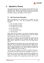
The operation theorem of the functions on the PCI-9812/10 card is
described in this chapter. The functions include A/D conversion
and digital input. The operation theorem would assist the user
understand, operate, and program the PCI-9812/10.
5.1 A/D Conversion Procedure
Before programming the PCI-9812/10 to perform the A/D
conversions, the user must first understand the following
concepts:
X
A/D conversion procedure
X
A/D signal source control
X
A/D trigger source control
X
A/D clock control
X
A/D data transfer mode
X
A/D data format
When using an A/D converter, users should be familiar with the
properties of the signal to be measured first. Users can decide
which channels to use and connect the signals to
PCI-9812/10. In addition, users should define and control the A/D
signal sources, including the A/D channels, A/D gains, and A/D
signal types. Please refer to section 5.2 for A/D signal source
control.
After deciding the A/D signal source, users must decide how to
trigger the A/D conversion and define/control the trigger source.
The A/D converter will start to convert the signal to a digital value
when a trigger condition is met. The PCI-9812/10 provides five
trigger modes please refer to section 5.3
The A/D clock is controlled by an internal or external clock source.
The operation of the A/D clock source is described in section 5.4.
At the end of an A/D conversion, the A/D data is buffered in a
FIFO. The total FIFO size on PCI-9812/10 is 32K samples. This
buffer size is relative to the highest data transfer rate. The A/D
Summary of Contents for NuDAQ PCI-9810
Page 4: ......
Page 10: ...vi ...
Page 19: ...Installation 9 2 3 PCI 9812 10 s Layout Figure 2 1 PCB Layout of the PCI 9812 10 ...
Page 22: ...12 ...
Page 40: ...30 ...
Page 78: ...68 Software Utility ...

