background image

ADLINK Technology Inc. 

LEC-

iMX6R2   User’s Guide


Page 38 

copyright © 2021 ADLINK Technology Inc.   


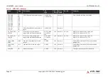
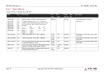
4.3.8.2


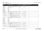
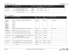
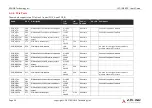
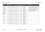
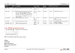
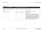
Second LAN port  

Second LAN port is derived from USB hub  
 

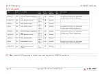
Name 

Pin # 

 Description   

 I/O  
Type  

I/O  
Level 

Power 
Domain 

PU / 
PD 

Comments 


GB 
GBE1_MDI0- 
GB 
GBE1_MDI1- 
GB 
GBE1_MDI2- 
GB 
GBE1_MDI3- 

S17 
S18 
S20 
S21 
S23 
S24 
S26 
S27 

Gigabit Ethernet Controller 1: Media Dependent 
Interface Differential Pairs 0, 1, 2, 3.  The MDI can 
operate in 1000, 100, and 10Mbit/sec modes.  Some 
pairs are unused in some modes according to the 
following: 
                        1000                     100          10       
MDI[0]+/-        B1_DA+/-             TX+/-       TX+/-  
MDI[1]+/-        B1_DB+/-             RX+/-       RX+/- 
MDI[2]+/-        B1_DC+/- 
MDI[3]+/-        B1_DD+/- 

GBE MDI    

Runtime 


Twisted pair signals for external 
transformer. 

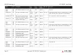
GBE1_LINK100# 

S19 

Link Speed Indication LED for GBE 1 100Mbps  

O OD  
CMOS  

3.3V  

Runtime 


Shall be able to sink 24mA or more Carrier 
LED current 

GBE1_LINK1000#  S22 

Link Speed Indication LED for GBE 1 1000Mbps  

O OD  
CMOS  

3.3V  

Runtime 


Shall be able to sink 24mA or more Carrier 
LED current 

GBE1_LINK_ACT#  S31 

Link / Activity Indication LED Driven low on Link (10, 100 
or 1000 mbps) Blinks on Activity  

O OD  
CMOS  

3.3V  

Runtime 


Shall be able to sink 24mA or more Carrier 
LED current 

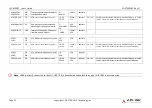
GBE1_CTREF 

S28 

Center-Tap reference voltage for Carrier board Ethernet 
magnetic `(if required by the Module GBE PHY)` 

Analog 

0 to 3.3V 
max 

Runtime 


GBE1_SDP 

P5 

IEEE 1588 Trigger Signal. For hardware implementation 
of PTP (precision time protocol) 

IO  
CMOS 

3.3V  

Runtime 


Summary of Contents for LEC-IMX6R2

Page 1: ...LEC IMX6R2 02 12 2021...

Page 2: ...descriptions at any time without notice Environmental Responsibility ADLINK is committed to fulfil its social responsibility to global environmental preservation through compliance with the European U...

Page 3: ...midity Keep equipment properly ventilated do not block or cover ventilation openings Make sure to use recommended voltage and power source settings Always install and operate equipment near an easily...

Page 4: ...INK Technology Inc LEC iMX6R2 User s Guide Page 4 copyright 2021 ADLINK Technology Inc Revision History Revision Description Date dd mm yyyy Author 1 0 Initial public release 10 03 2021 Henri Parmenti...

Page 5: ...9 Boot Modes 15 2 10 Power 16 2 11 Mechanical and Environmental 16 3 Block Diagram 17 4 Pinout and Signal Descriptions 18 4 1 Pin Summary 18 4 2 Signal Terminology Descriptions 22 4 3 Signal Descripti...

Page 6: ...AN bus 45 4 4 4 Miscellaneous 45 4 4 5 Power and System Management 46 4 4 6 DB30 Multipurpose Connector 47 4 4 7 Boot Select 48 4 4 8 Power 49 4 5 SMARC pin to controller mapping 50 5 Software Support...

Page 7: ...LEC iMX6R2 User s Guide SGET SMARC Rev 2 1 Page 7 copyright 2021 ADLINK Technology Inc List of Figures Figure 1 Module function diagram 17 Figure 2 Module top botom side pin numbering 18...

Page 8: ...The Module PCBs have 314 edge fingers that mate with a low profile 314 pin 0 5 mm pitch right angle connector the connector is sometimes identified as a 321 pin connector but 7 pins are lost to the k...

Page 9: ...s industrial 40 C to 85 C or commercial 0 C to 70 C type L2 Cache 32 KB I cache 32 KB D cache Memory 512MB 1 2 4GB DDR3L memory down IoT security CryptoAuthentication Device Microchip ATECC608A Crypto...

Page 10: ...k datasheet for more info GPU VPU Feature Support Video 2D and 3D Graphics Units integrated in i MX6 Processor OpenGL ES 1 1 2 0 Halti OpenVG 1 1 OpenCL 1 1 EP Multi Format Hardware Video Encoder Deco...

Page 11: ...MX6R2 User s Guide SGET SMARC Rev 2 1 Page 11 copyright 2021 ADLINK Technology Inc Camera support Single MIPI CSI camera supported on CSI1 Four lanes QuadPlus Quad DualPlus Dual Two lanes DualLite and...

Page 12: ...module through RGMII Operates on TCP IP UDP IP and ICMP IP protocol data or on IP header only NOTE The Ethernet throughput is limited to 400 Mbit s by the Freescale SoC Optional Secondary LAN MAC PHY...

Page 13: ...d SER2 TX X CTS RTS 7 or 8 bit data words 1 or 2 stop bits programmable parity even odd or none Programmable baud rates up to 5 MHz 32 byte FIFO on Tx and 32 half word FIFO on Rx supporting auto baud...

Page 14: ...s and 1 Mbit s General Purpose I2C_GP for usage on carrier Power Management I2C_PM connected to PMIC LCD I2C to detect and manage connected displays Camera I2C GPIO 12x GPIO with interrupt 2 6 System...

Page 15: ...toring boot configuration logistics and forensic information flat panel control watchdog timer 2 8 Debug Header 30 pin multipurpose flat cable connector for use with optional DB 30 debug module Provid...

Page 16: ...SMARC Specifications v2 1 Dimension SMARC small size module 82mm x 50mm Operating Temperature Standard 0 C to 60 C Rugged 40 C to 85 C optional Humidity 5 90 RH operating non condensing 5 95 RH storag...

Page 17: ...B1 USB2 USB3 USB4 LAN1 LAN0 PCIe0 CAN0 CAN1 SPI0 SPI1 UART0 UART1 UART2 UART3 I2S0 SDIO GPIO I2C_GP I2C_PM NXP iMX6 SMARC REV 2 1 USB 2 0 OTG USB 2 0 Host MIPI CSI 2 lanes Dual Channel LVDS DSI 2 lane...

Page 18: ...ns 4 1 Pin Summary The below table is a comprehensible list of all signal pins on the MXM 3 connector in the standard specification SMARC 2 1 Those signals not supported on LEC iMX6R2 are strikethroug...

Page 19: ...P31 SPI0_CS1 note 2 S32 PCIE_D_RX SERDES_1_RX P32 GND S33 PCIE_D_RX SERDES_1_RX P33 SDIO_WP S34 GND P34 SDIO_CMD S35 USB4 P35 SDIO_CD S36 USB4 P Pin Primary Top Side S Pin Secondary Bottom Side P36 S...

Page 20: ..._HPD DP1_HPD S105 DP0_AUX P105 HDMI_CTRL_CK DP1_AUX S106 DP0_AUX P106 HDMI_CTRL_DAT DP1_AUX S107 LCD1_BKLT_EN P107 DP1_AUX_SEL S108 LVDS1_CK eDP1_AUX DSI1_CLK P108 GPIO0 CAM0_PWR S109 LVDS1_CK eDP1_AU...

Page 21: ...PD DSI0_TE P144 CAN0_RX S145 WDT_TIME_OUT P145 CAN1_TX S146 PCIE_WAKE P146 CAN1_RX S147 VDD_RTC P147 VDD_IN S148 LID P148 VDD_IN S149 SLEEP P Pin Primary Top Side S Pin Secondary Bottom Side P149 VDD_...

Page 22: ...gnal for MIPI CSI 2 cameras and DSI displays LVDS M PHY Low Voltage Differential Signal for MIPI CSI 3 cameras LVDS LCD Low Voltage Differential Signal for LCD displays LVDS PCIE Low Voltage Different...

Page 23: ...S0_2 LVDS0_2 LVDS0_3 LVDS0_3 DSI0_D0 DSI0_D0 DSI0_D1 DSI0_D1 DSI0_D2 DSI0_D2 DSI0_D3 DSI0_D3 eDP0_TX0 eDP0_TX0 eDP0_TX1 eDP0_TX1 eDP0_TX2 eDP0_TX2 eDP0_TX3 eDP0_TX3 S111 S112 S114 S115 S117 S118 S120...

Page 24: ..._BKLT_EN S127 Primary LVDS channel backlight enable active high O CMOS 1 8V Runtime LCD0_BKLT_PWM S141 Primary LVDS channel brightness control through pulse width modulation PWM O CMOS 1 8V Runtime LV...

Page 25: ...137 S138 Primary DSI panel differential pair data lines O LVDS D PHY Runtime Build option DSI0_CLK DSI0_CLK S134 S135 Primary DSI panel differential pair clock lines O LVDS D PHY Runtime Build option...

Page 26: ...HDMI_D0 DP1_LANE0 DP1_LANE0 DP1_LANE1 DP1_LANE1 DP1_LANE2 DP1_LANE2 P101 P102 HDMI_CK HDMI_CK DP1_LANE3 DP1_LANE3 S105 HDMI_CTRL_CK DP1_AUX S106 HDMI_CTRL_DAT DP1_AUX P104 HDMI_HPD DP1_HPD P107 DP1_AU...

Page 27: ...air clock lines O TMDS HDMI Runtime AC coupled off module HDMI_CTRL_CK P105 I2C_CLK line dedicated to HDMI O OD COMS 1 8V Runtime PU 2 2 Level shifter FET and 5V PU resistor shall be placed between th...

Page 28: ...T CSI0_TX S7 I2C data for serial camera data support link or differential data lane I O OD CMOS O LVDS M PHY 1 8V Runtime PU 2 2K MIPI CSI 2 0 uses I2C_CAM0_DAT MIPI CSI 3 0 uses CSI0_TX I2C_CAM0_CK C...

Page 29: ...al camera data support link or differential data lane I O OD CMOS O LVDS M PHY 1 8V Runtime PU 2 2K MIPI CSI 2 0 mode uses I2C_CAM1_DAT MIPI CSI 3 0 mode uses CSI1_TX I2C_CAM1_CK CSI1_TX S1 I2C clock...

Page 30: ...ck I O CMOS 1 8V Runtime Module Output if CPU acts in Master Mode Module Input if CPU acts in Slave Mode I2S2_LRCK S50 I2S2 Left Right synchronization clock I O CMOS 1 8V Runtime Module Output if CPU...

Page 31: ...LEC iMX6R2 User s Guide SGET SMARC Rev 2 1 Page 31 copyright 2021 ADLINK Technology Inc 4 3 5 USB ports...

Page 32: ...port 1 I O USB USB Runtime From USB HUB USB1_EN_OC P67 USB over current sense for port 1 I O OD CMOS 3 3Vsb 3 3V Runtime PU 10k Pulled low by Module OD driver to disable USB0 power Pulled low by Carr...

Page 33: ...announce OTG device insertion on USB 3 0 port I CMOS 3 3Vsb 3 3V Runtime USB4 USB4 S35 S36 USB differential data pairs for port 4 I O USB USB Runtime USB4_EN_OC P76 USB over current sense for port 4...

Page 34: ...nboard PCIe clock PCIE_B_TX PCIE_B_TX S90 S91 Differential PCIe link B transmit data pair O LVDS PCIE Runtime Series AC coupled on module PCIE_B_RX PCIE_B_RX S87 S88 Differential PCIe link B receive d...

Page 35: ...nk D transmit data pair O LVDS PCIE Runtime Series AC coupled on module PCIE_D_RX PCIE_D_RX S32 S33 Differential PCIe link D receive data pair I LVDS PCIE Runtime Series AC coupled off module PCIE_WAK...

Page 36: ...s SATA0_TX SATA0_TX P48 P49 Serial ATA channel 0 Transmit Output differential pair O SATA Runtime Series AC coupled on Module 10 nF SATA0_RX SATA0_RX P51 P52 Serial ATA channel 0 Receive Input differe...

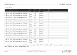
Page 37: ...RX MDI 2 B1_DC MDI 3 B1_DD GBE MDI Runtime Twisted pair signals for external transformer GBE0_LINK100 P21 Link Speed Indication LED for GBE 0 100Mbps O OD CMOS 3 3V Runtime Shall be able to sink 24mA...

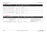
Page 38: ...DI 3 B1_DD GBE MDI Runtime Twisted pair signals for external transformer GBE1_LINK100 S19 Link Speed Indication LED for GBE 1 100Mbps O OD CMOS 3 3V Runtime Shall be able to sink 24mA or more Carrier...

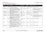
Page 39: ...Response This signal is used for card initialization and for command transfers During initialization mode this signal is open drain During command transfer this signal is in push pull mode I O CMOS 1...

Page 40: ...CMOS 1 8V Standby also referred to as MISO SPI0_DO P46 SPI0 Master output Slave input O CMOS 1 8V Standby also referred to as MOSI SPI1_CS0 P54 SPI1 Master Chip Select 0 O CMOS 1 8V Standby See ESPI...

Page 41: ...ERT0 ESPI_ALERT1 S43 S44 ESPI ALERT I OD CMOS 1 8V Standby This pin is used by eSPI slave to request service from eSPI master Alert is an open drain output from the slave This pin is optional for Sing...

Page 42: ...a single big list Below is an overview of all I2C busses and where to find them Name Pin Description Where to find I2C_LCD_DAT S140 DDC data line used for flat panel detection and control LVDS DSI eD...

Page 43: ...8V Runtime PU 470K on the Module Default use is GPIO3 alternative use is Camera 1 Reset active low through DTS GPIO4 HDA_RST P112 General purpose I O pin 4 I O CMOS 1 8V Runtime PU 470K on the Module...

Page 44: ...CMOS 1 8V Runtime SER1_RX P135 Asynchronous serial data input port 1 I CMOS 1 8V Runtime SER2_TX P136 Asynchronous serial data output port 2 O CMOS 1 8V Runtime SER2_RX P137 Asynchronous serial data i...

Page 45: ...utput O CMOS 1 8V Runtime CAN1_RX P146 CAN port1 Receive input I CMOS 1 8V Runtime 4 4 4 Miscellaneous Name Pin Description I O Type I O Level Power Domain PU PD Comments TEST S157 Held low by Carrier...

Page 46: ...Carrier to float the line when charge is complete I OD CMOS 1 8 to 5V Standby Sleep PU 10k Driven by OD on Carrier VIN_PWR_BAD S150 Power bad indication from Carrier Board Module and Carrier power sup...

Page 47: ...an edge triggered signal I OD CMOS 1 8 to 5V Standby PU 10k Driven by OD on Carrier I2C_PM_DAT P122 Power management I2C bus DATA I O OD CMOS 1 8V Runtime PU 2k2 On x86 systems these serve as SMB DATA...

Page 48: ...OS 1 8Vsb Standby PU 10K Driven by OD on Carrier Pulled up on module Low on this pin allows non protected segments of Module boot device to be rewritten restored from an external USB Host on Module US...

Page 49: ...ltage 4 75 min to 5 25V max 3 to 5 25V 5V GND P2 P9 P12 P15 P18 P32 P38 P47 P50 P53 P59 P68 P79 P82 P85 P88 P91 P94 P97 P100 P103 P120 P133 P142 S3 S10 S16 S25 S34 S47 S61 S64 S67 S70 S73 S80 S83 S86...

Page 50: ...MX6 QP Q DP D DL S CSI_D1M NVCC_MIPI P12 GND P13 CSI1_RX2 In LVDS D PHY i MX6 QP Q DP D CSI_D2P NVCC_MIPI P14 CSI1_RX2 In LVDS D PHY i MX6 QP Q DP D CSI_D2M NVCC_MIPI P15 GND P16 CSI1_RX3 In LVDS D P...

Page 51: ...0 NVCC_SD2 P43 SPI0_CS0 Out CMOS 1 8V i MX6 QP Q DP D DL S DISP0_DAT3 Alt2 NVCC_LCD P44 SPI0_CK Out CMOS 1 8V i MX6 QP Q DP D DL S DISP0_DAT0 Alt2 NVCC_LCD P45 SPI0_DIN In CMOS 1 8V i MX6 QP Q DP D DL...

Page 52: ...n PU 10K CMOS 3 3V LAN9514 JZX PRTCTL4 P75 PCIE_A_RST Out CMOS 3 3V i MX6 QP Q DP D DL S GPIO_17 Alt5 NVCC_GPIO P76 USB4_EN_OC In PU 10K CMOS 3 3V LAN9514 JZX PRTCTL5 P77 PCIE_B_CKREQ P78 PCIE_A_CKREQ...

Page 53: ...9 GPIO1 CAM1_PWR Out PU 470K CMOS 1 8V i MX6 QP Q DP D DL S DISP0_DAT13 Alt5 NVCC_LCD P110 GPIO2 CAM0_RST Out CMOS 1 8V i MX6 QP Q DP D DL S DISP0_DAT12 Alt5 NVCC_LCD P111 GPIO3 CAM1_RST Out PU 470K C...

Page 54: ...NVCC_GPIO P137 SER2_RX Out CMOS 1 8V i MX6 QP Q DP D DL S KEY_ROW1 Alt4 NVCC_GPIO P138 SER2_RTS In CMOS 1 8V i MX6 QP Q DP D DL S KEY_COL4 Alt4 NVCC_GPIO P139 SER2_CTS Out CMOS 1 8V i MX6 QP Q DP D DL...

Page 55: ...14 CSI0_RX1 S15 CSI0_RX1 S16 GND S17 GBE1_MDI0 Bi Dir PU 49 9R RGMII LAN9514 JZX TXP S18 GBE1_MDI0 Bi Dir PU 49 9R RGMII LAN9514 JZX TXN S19 GBE1_LINK100 Out serial 0R RGMII LAN9514 JZX nSPD_LED GPIO2...

Page 56: ...L S CSI0_DAT7 Alt4 NVCC_CSI S42 I2S0_CK Bi Dir CMOS 1 8V i MX6 QP Q DP D DL S CSI0_DAT4 Alt4 NVCC_CSI S43 ESPI_ALERT0 S44 ESPI_ALERT1 S45 MDIO_CLK S46 MDIO_DAT S47 GND S48 I2C_GP_CK Out PU 2 2K I2C3 i...

Page 57: ..._SSTX S73 GND S74 USB2_SSRX S75 USB2_SSRX S76 PCIE_B_RST S77 PCIE_C_RST S78 PCIE_C_RX SERDES_2_RX S79 PCIE_C_RX SERDES_2_RX S80 GND S81 PCIE_C_TX SERDES_2_TX S82 PCIE_C_TX SERDES_2_TX S83 GND S84 PCIE...

Page 58: ...VDS1_0 eDP1_TX0 DSI1_D0 Out LVDS i MX6 QP Q DP D DL S LVDS1_TX0_N NVCC_LVDS_2P5 S113 eDP1_HPD DSI1_TE S114 LVDS1_1 eDP1_TX1 DSI1_D1 Out LVDS i MX6 QP Q DP D DL S LVDS1_TX1_P NVCC_LVDS_2P5 S115 LVDS1_1...

Page 59: ...DP0_AUX DSI0_CLK Out serial 0R LVDS i MX6 QP Q DP D DL S LVDS0_CLK_P NVCC_LVDS_2P5 S135 LVDS0_CK eDP0_AUX DSI0_CLK Out serial 0R LVDS i MX6 QP Q DP D DL S LVDS0_CLK_N NVCC_LVDS_2P5 S136 GND S137 LVDS0...

Page 60: ...CMOS 1 8V i MX6 QP Q DP D DL S NANDF_D6 Alt5 NVCC_NANDF S153 CARRIER_STBY Out CMOS 1 8V BMC PB1 S154 CARRIER_PWR_ON_B BMC Out CMOS 1 8V BMC PB6 S155 FORCE_RECOV_B In PU 4 7K CMOS 1 8V i MX6 QP Q DP D...

Page 61: ...ftware Support 5 1 1 Uboot Yocto Goto https github com adlink Yocto source code and compiling instructions are available 5 1 2 Ubuntu Build instruction from source are available on Github 5 1 3 Androi...

Page 62: ...ADLINK Technology Inc LEC iMX6R2 User s Guide Page 62 copyright 2021 ADLINK Technology Inc 6 Mechanical...

Page 63: ...LEC iMX6R2 User s Guide SGET SMARC Rev 2 1 Page 63 copyright 2021 ADLINK Technology Inc 7 Thermal Solutions 7 1 1 Heatsink THS 4 74 4 34 82 42 3 12 2 7mm x 4pcs...

Page 64: ...74 82 42 3 6 2 7mm x 4pcs M3 x 4pcs 7 1 2 Heatspreader HTS THS HTS sIMX6R2 SDL Heatspreader for LEC iMXR2 solo Duallite THS sIMX6R2 SDL Low profile heatsink for LEC iMX6R2 Solo DualLite HTS sIMX6R2 D...

Page 65: ...LEC iMX6R2 User s Guide SGET SMARC Rev 2 1 Page 65 copyright 2021 ADLINK Technology Inc...

Reviews: