background image


Leading

EDGE COMPUTING


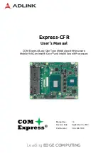
Express-CFR 

User’s Manual


COM Express Basic Size Type 6


Module with Hexa-core  

Mobile 9th Gen Intel® Core™ and Intel® Xeon® Processors


Manual Rev.:    

1.0 

Revision Date:    

September 30, 2019 

Part Number:    

50-1J099-1000 

Summary of Contents for COM Express Express-CFR

Page 1: ...COMPUTING Express CFR User s Manual COM Express Basic Size Type 6 Module with Hexa core Mobile 9th Gen Intel Core and Intel Xeon Processors Manual Rev 1 0 Revision Date September 30 2019 Part Number 5...

Page 2: ...al protection is a top priority for ADLINK We have enforced measures to ensure that our products manufacturing processes components and raw materials have as little impact on the environment as possib...

Page 3: ...ental 6 2 15 Specification Compliance 6 2 16 Operating Systems 6 2 17 Functional Diagram 7 2 18 Mechanical Drawing 8 3 Pinouts and Signal Descriptions 9 3 1 AB CD Pin Definitions 9 3 2 Signal Descript...

Page 4: ...u Structure 53 7 2 Main 54 7 3 Advanced 56 7 4 Chipset 69 7 5 Security 80 7 6 Boot 83 7 7 Save Exit 84 8 BIOS Checkpoints Beep Codes 85 8 1 Status Code Ranges 86 8 2 Standard Status Codes 86 8 3 OEM R...

Page 5: ...gram 7 Figure 2 Express CFR Mechanical Drawing 8 Figure 3 Express CFR Connector Switch and LED Locations 33 Figure 4 Express CFR and the DB40 Debug Module 34 Figure 5 Express CFR Switch Locations 39 F...

Page 6: ...able 3 Express CFR LED Descriptions 36 Table 4 Fan Connector Pin Definition 37 Table 5 PCI Express Configuration Switch Settings 39 Table 6 BIOS Select and Mode Configuration Switch Settings 40 Table...

Page 7: ...1 2 0 1 2 Intel Clear Video HD Technology Advanced Scheduler 2 0 1 0 XPDM support and DirectX Video Acceleration DXVA support for full H 265 HEVC 10 bit MPEG2 hardware codec In addition High Dynamic...

Page 8: ...2 Introduction This page intentionally left blank...

Page 9: ...Device Protection Technology with Intel Secure Key Intel TSXNI availability of features may vary between processor SKUs Cache 12MB for Xeon 9MB for Core i7 8MB for Core i5 6MB for Core i3 Memory 2133...

Page 10: ...ing HEVC H 265 10 bit H 264 M JPEG MPEG2 VC1 WMV9 VP9 10 bit HW decode HEVC H 265 10 bit M JPEG MPEG2 HW encode Advanced Scheduler 2 0 1 0 XPDM support DirectX up to 12 OpenGL up to 4 5 OpenCL up to 2...

Page 11: ...table in BIOS COM Port Description IRQ Address Console redirection support COM 1 Supported by module SER0 A98 A99 via NCT5104D 4 0x3F8 Yes COM 2 Supported by module SER1 A101 A102 via NCT5104D 3 0x2F8...

Page 12: ...p S5 for 5Vsb power saving 2 12 Power Consumption Please contact your ADLINK representative for the document COM Express Module Power Consumption 2 13 Operating Temperatures Standard Operating Tempera...

Page 13: ...x USB 3 1 port 0 1 2 3 UART0 1 SPI 1 BIOS DDC I2C SODIMM 2 2133 2400 MHz 4 32 GB DDR4 2x PCIe x1 Gen3 port 6 7 SPI_CS DDI 1 DP HDMI DVI DDI 2 DP HDMI DVI DDI 3 DP HDMI DVI single dual 18 24 bit LVDS 6...

Page 14: ...dimensions shown in millimeters Tolerances should be 0 25mm 0 010 unless otherwise noted The tolerances of the module connector locating peg holes dimensions 16 50 6 00 and 16 50 18 00 should be 0 10...

Page 15: ...RBTN C12 USB_SSRX3 D12 USB_SSTX3 A13 GBE0_MDI0 B13 SMB_CK C13 USB_SSRX3 D13 USB_SSTX3 A14 GBE0_CTREF B14 SMB_DAT C14 GND D14 GND A15 SUS_S3 B15 SMB_ALERT C15 DDI1_PAIR6 D15 DDI1_CTRLCLK_AUX A16 SATA0_...

Page 16: ...4 GPI0 B54 GPO1 C54 TYPE0 D54 PEG_LANE_RV A55 PCIE_TX4 B55 PCIE_RX4 C55 PEG_RX1 D55 PEG_TX1 A56 PCIE_TX4 B56 PCIE_RX4 C56 PEG_RX1 D56 PEG_TX1 A57 GND B57 GPO2 C57 TYPE1 D57 TYPE2 A58 PCIE_TX3 B58 PCIE...

Page 17: ...3 A95 SPI_MOSI B95 VGA_I2C_CK C95 PEG_RX13 D95 PEG_TX13 A96 TPM_PP B96 VGA_I2C_DAT C96 GND D96 GND A97 TYPE10 B97 SPI_CS C97 RSVD D97 RSVD A98 SER0_TX B98 RSVD C98 PEG_RX14 D98 PEG_TX14 A99 SER0_RX B9...

Page 18: ...O 5V Output 5V signal level I O 3 3V Bi directional signal 3 3V tolerant I O 5V Bi directional signal 5V tolerant I O 3 3Vsb Input 3 3V tolerant active in standby state P Power Input Output REF Refere...

Page 19: ...monitor Analog DAC output designed to drive a 37 5 Ohm equivalent load O Analog PD 150R shall also be terminated on the carrier with 150 resistor to ground close to VGA connector VGA_GRN B91 Green fo...

Page 20: ...B3 B71 B72 B73 B74 B75 B76 B77 B78 LVDS Channel B differential pairs O LVDS LVDS_B_CK LVDS_B_CK B81 B82 LVDS Channel B differential clock O LVDS LVDS is default support LVDS_VDD_EN A77 LVDS panel powe...

Page 21: ...e in 1000 100 and 10Mbit sec modes Some pairs are unused in some modes according to the following 1000 100 10 MDI 0 B1_DA TX TX MDI 1 B1_DB RX RX MDI 2 B1_DC MDI 3 B1_DD I O Analog Twisted pair signal...

Page 22: ...r I SATA AC coupled on Module SATA2_TX SATA2_TX A22 A23 Serial ATA channel 2 Transmit Output differential pair O SATA AC coupled on Module SATA2_RX SATA2_RX A25 A26 Serial ATA channel 2 Receive Input...

Page 23: ...nsmit Output differential pair O PCIE AC coupled on Module PCIE_RX3 PCIE_RX3 B58 B59 PCI Express channel 3 Receive Input differential pair I PCIE AC coupled off Module PCIE_TX4 PCIE_TX4 A55 A56 PCI Ex...

Page 24: ...ddress command and data bus I O 3 3V LPC_FRAME B3 LPC frame indicates the start of an LPC cycle O 3 3V LPC_DRQ0 LPC_DRQ1 B8 B9 LPC serial DMA request I 3 3V NC pins LPC_SERIRQ A50 LPC serial interrupt...

Page 25: ...current monitor on the carrier board may drive this line low I 3 3VSB PU 10K 3 3VSB Do not pull high on carrier USB_2_3_OC A44 USB over current sense USB ports 2 and 3 A pull up for this line shall be...

Page 26: ...from module to carrier board SPI BIOS flash O 3 3VSB SPI_CLK A94 Clock from module to carrier board SPI BIOS flash O 3 3VSB SPI_POWER A91 Power supply for Carrier Board SPI sourced from Module nominal...

Page 27: ...sed to indicate Physical Presence to the TPM I 3 3V PD 100K PD only when TPM on module Modules implementing a TPM shall pull down TPM_PP 3 3 13 SMBus Signal Pin Description I O PU PD Comment SMB_CK B1...

Page 28: ...internally on the module I 3 3V PU 10K 3 3V GPI 2 A67 General purpose input pins Pulled high internally on the module I 3 3V PU 10K 3 3V GPI 3 A85 General purpose input pins Pulled high internally on...

Page 29: ...sed to notify LPC devices O 3 3VSB SUS_S3 A15 Indicates system is in Suspend to RAM state Active low output An inverted copy of SUS_S3 on the carrier board also known as PS_ON may be used to enable th...

Page 30: ...section 7 Electrical Specifications for allowable input range If VCC5_SBY is used all available VCC_5V_SBY pins on the connector s shall be used Only used for standby and suspend functions May be left...

Page 31: ...erSpeed USB data path on USB2 I PCIE AC coupled off module USB_SSTX2 USB_SSTX2 D9 D10 Additional Transmit signal differential pairs for the SuperSpeed USB data path on USB2 O PCIE AC coupled on module...

Page 32: ...SEL is floating I O PCIE PD 100K AC couple on Module DP1_AUX DDI1_CTRLCLK_AUX D15 If DDI1_DDC_AUX_SEL pulled high I O OD 3 3V HDMI1_CTRLCLK PU 2 2K 3 3V when DDC_AUX_SEL is high If DDI1_DDC_AUX_SEL is...

Page 33: ...DDI2_DDC_AUX_SEL pulled high I O OD 3 3V HDMI2_CTRLCLK PU 2 2K 3 3V when DDC_AUX_SEL is high If DDI2_DDC_AUX_SEL is floating I O PCIE PU 100K 3 3V AC couple on Module DP2_AUX DDI2_CTRLDATA_AUX C33 If...

Page 34: ...DC_AUX_SEL pulled high I O OD 3 3V HDMI2_CTRLCLK PU 2 2K 3 3V when DDC_AUX_SEL is high If DDI3_DDC_AUX_SEL is floating I O PCIE PU 100K 3 3V AC couple on Module DP2_AUX DDI3_CTRLDATA_AUX C37 If DDI3_D...

Page 35: ...ANE0 TMDS2_DATA2 D40 DDI2_PAIR0 DP2_LANE0 TMDS2_DATA2 D42 DDI2_PAIR1 DP2_LANE1 TMDS2_DATA1 D43 DDI2_PAIR1 DP2_LANE1 TMDS2_DATA1 D46 DDI2_PAIR2 DP2_LANE2 TMDS2_DATA0 D47 DDI2_PAIR2 DP2_LANE2 TMDS2_DATA...

Page 36: ...99 C101 C102 PCI Express Graphics transmit differential pairs I PCIE AC couple off module PEG_TX0 PEG_TX0 PEG_TX1 PEG_TX1 PEG_TX2 PEG_TX2 PEG_TX3 PEG_TX3 PEG_TX4 PEG_TX4 PEG_TX5 PEG_TX5 PEG_TX6 PEG_TX...

Page 37: ...ement combinatorial logic that monitors the module TYPE pins and keeps power off e g deactivates the ATX_ON signal for an ATX power supply if an incompatible module pin out type is detected The Carrie...

Page 38: ...32 Pinouts and Signal Descriptions This page intentionally left blank...

Page 39: ...s that are used on the module but are not included in the PICMG standard specification 4 1 Connector Switch and LED Locations 40 pin Multi Purpose CD AB Fan 4 pin Fan BIOS Defaults Reset Switch CD AB...

Page 40: ...34 Connector Pinouts on Module Express CFR and the DB40 Debug Module For illustration purposes only Figure 4 Express CFR and the DB40 Debug Module...

Page 41: ...wer 3 3V provide from COM module 28 BMC Program interface cont d OCD0B Include a jumper to connect OCD0A via 1K0 pull up to 3 3V_BMC 9 GND 29 PWRBTN 10 BIOS_DIS0 30 SYS_RESET 11 RST 31 CB_RESET 12 CLK...

Page 42: ...een Power Source 3Vcc S0 LED ON S3 S4 S5 LED OFF ECO mode LED OFF LED3 Red BMC output and same signal as WDT B27 on BtB connector Module power up WD LED LED OFF Watchdog counting WD LED Keep Last Stat...

Page 43: ...nnector Pinouts on Module 37 4 4 Fan Connector Connector Type JVE 24W1125A 04M00 Pin Orientation 1 2 3 4 Pin Assignment Name Description 1 FAN_PWMOUT 2 FAN_TACHIN 3 Ground 4 5V Table 4 Fan Connector P...

Page 44: ...perform the following steps 1 Shut down the system 2 Press the BIOS Setup Defaults RESET Button continuously and boot up the system You can release the button when the BIOS prompt screen appears 3 The...

Page 45: ...tions 4 6 1 PCI Express Configuration Switch PCI Express Configuration Switch also referred to as the PEG config switch allows you to configure the PCI Express x16 lanes from the CPU as 1 PCIe x16 2 P...

Page 46: ...lsafe mode both BIOS chips on the module are configured as SPI1 Only one of the two is connected to the SPI bus at any given time In case of failure of the primary SPI1 BIOS the system will reboot and...

Page 47: ...ion of the CPU s PEG interface PCIe x16 The card reroutes the PCIe x16 to two x8 and allows testing of two independent PCIe add on cards with x8 x4 x2 x1 width To use the card set BIOS Advanced Graphi...

Page 48: ...42 Connector Pinouts on Module This page intentionally left blank...
Page 49: ...are stored in flash Power cycles counter Boot counter Counts the number of boot attempts Watchdog Timer Set Reset Disable Watchdog Timer Features auto reload at power up System Restart Cause Power los...

Page 50: ...3 3 1024 9 VCCIO MSB 8 LSB x 1 x 3 3 1024 10 VCCSTG MSB 8 LSB x 1 x 3 3 1024 11 VCCSA MSB 8 LSB x 1 x 3 3 1024 12 1V8_A MSB 8 LSB x 1 x 3 3 1024 13 V5SBY MSB 8 LSB x 1 826 x 3 3 1024 14 V12 MSB 8 LSB...

Page 51: ...es a blinking code on the blue Status LED LED1 The same error code is also reported by the BMC Flags register The Exception Code is not stored in the Flash Storage and is cleared when the power is rem...

Page 52: ...O_P_5V_3V3_S0_PG Table 9 SEMA Exception Codes 5 1 5 BMC Flags The BMC Flags register returns the last detected Exception Code since power up and shows the BIOS in use and the power mode Bit Descriptio...

Page 53: ...000A0000 000BFFFF PCI Express Root Complex 6 2 I O Map Hex Range Device 20h 21h Interrupt Controller 24h 25h Interrupt Controller 28h 29h Interrupt Controller 2Ch 2Dh Interrupt Controller 2E 02F Moth...

Page 54: ...ns Port COM1 4D0h 4D1h Interrupt Controller 680h 69Fh Motherboard resources 6A0h Motherboard resources CF9h Reset Generator 6 3 Interrupt Request IRQ Lines PIC Mode IRQ Typical Intterupt Resource Conn...

Page 55: ...Serial Port 1 COM1 IRQ4 via SERIRQ Note 1 5 Serial Port 3 COM3 IRQ5 via SERIRQ Note 1 6 N A N A Note 1 7 Serial Port 4 COM4 IRQ7 via SERIRQ Note 1 8 Real time clock N A No 9 N A N A Note 1 10 N A N A...

Page 56: ...Interface 00h 16h 03h Internal Intel Active Management Technology SOL 00h 17h 00h Internal Intel AHCI controller 00h 1Bh 00h Internal Intel PCI Express Root port 5 00h 1Bh 01h Internal Intel PCI Expre...

Page 57: ...NTC 18 Int3 INTD 19 INTD 19 INTD 19 INT Line PCIE Port1 PCIE Port 2 PCIE Port 3 PCIE Port 4 PCIE Port 5 PCIE Port 6 PCIE Port 7 PCIE Port 8 Int0 INTA 16 INTB 17 INTC 18 INTD 19 INTA 16 INTB 17 INTC 18...

Page 58: ...52 System Resources This page intentionally left blank...

Page 59: ...he respective table Main Advanced Chipset Security Boot Save Exit BIOS Information System Information Board Information System Date System Time CPU Configuration Graphics Configuration Power Managemen...

Page 60: ...ation Board Information Info only Description Project Name Info only Display Project Name CPU Board Version Info only Display CPU signature CPU Brand String Info only Display CPU brand name Stepping I...

Page 61: ...he returned value specifies the number of times the external power supply has been shut down Boot Cycles Read only The Bootcounter is increased after a HW or SW Reset or after a successful power up Bo...

Page 62: ...t optimized for Hyper Threading Technology Intel R SpeedStep tm Disabled Enabled Allows more than two frequency ranges to be supported Intel R Speed Shift Technology Disabled Enabled Enable Disable In...

Page 63: ...led VT d capability DTS SMM Disabled Enabled Critical Temp Reporting Out of spec Disabled ACPI thermal management uses EC reported temperature values Enabled ACPI thermal management uses DTS SMM mecha...

Page 64: ...ith HDMI DVI Compatible Set DDI port 2 function to DisplayPort or HDMI DDI port 3 No Device Display Port HDMI DisplayPort with HDMI DVI Compatible Set DDI port 3 function to DisplayPort or HDMI Note D...

Page 65: ...turned on Remain off To start the machine the power button has to pressed Last State The machine will power up to last power state Power Consumption Submenu 7 3 3 1 Power Management Power Consumption...

Page 66: ...vice USB Port Disable Override Disabled Select Per Pin Selectively Enable Disable the corresponding USB port from reporting a Device Connection to the controller 7 3 5 AMT Configuration Feature Option...

Page 67: ...Temperature Info only Current Read only Startup Read only Min Read only Max Read only Board Temperatures Info only Current Read only Startup Read only Min Read only Max Read only CPU Fan Speed Read o...

Page 68: ...ly Trigger Temperature 85 Trigger Temperature PWM Level 100 PWM Level 7 3 8 Watchdog Timer Feature Options Description Watchdog Timer Info only Power Up watchdog Disabled Enabled The Power Up Watchdog...

Page 69: ...6 7 10 11 12 IO 250h IRQ 3 4 5 6 7 10 11 12 IO 258h IRQ 3 4 5 6 7 10 11 12 IO 260h IRQ 3 4 5 6 7 10 11 12 IO 268h IRQ 3 4 5 6 7 10 11 12 Enable or Disable Serial Port COM Fixed configuration of serial...

Page 70: ...of serial port Select an optimal setting for Super IO device 7 3 9 4 NCT5104D Super IO Configuration Serial Port 2 Configuration Feature Options Description Serial Port 2 Configuration Info only Seri...

Page 71: ...port transmission speed The speed must be matched on the other side Long or noisy lines may require lower speeds Data Bits 7 8 Data Bits Parity None Even Odd Mark Space A parity bit can be sent with t...

Page 72: ...mns supported redirection Redirect After POST Always Enable BootLoader When Bootloader is selected then Legacy Console Redirection is disabled before booting to legacy OS When Always Enable is selecte...

Page 73: ...e Platform Hierarchy Storage Hierarchy Disabled Enabled Enable or Disable Storage Hierarchy Endorsement Hierarchy Disabled Enabled Enable or Disable Endorsement Hierarchy TPM2 0 UEFI Spec Version TCG_...

Page 74: ...able IPv6 PXE Support Disabled Enabled Enable Disable IPv6 PXE boot support If disabled IPv6 PXE boot support will not be available IPv6 HTTP Support Disabled Enabled Enable Disable IPv6 HTTP boot sup...

Page 75: ...set System Agent SA Configuration Feature Options Description System Agent SA Configuration Info only SA PCIe Code Version Read only VT d Read only Memory Configuration Submenu Graphics Configuration...

Page 76: ...00 3400 3467 3600 3733 3800 4000 4200 4267 4400 4533 4600 4800 5000 5067 5200 5333 5400 5600 5800 5867 6000 6133 6200 Maximum Memory Frequency Selections in MHz Valid values should match the refclk i...

Page 77: ...r Enable to dGPU Elk Creek 4 DGPU Power Enable ActiveLow PEG Eval DGPU Power Enable ActiveHigh Internal Graphics Auto Disabled Enabled Keep IGFX enabled based on the setup options GTT Size 2MB 4MB 8MB...

Page 78: ...r attached to this Port The number has to be globally unique within the chassis Values 0 8191 PEG 0 1 1 Read only Enable Root Port Disabled Enabled Auto Enable or Disable the Root Port Max Link Speed...

Page 79: ...for the Slot Power Limit Value PEG0 Physical Slot Number 3 Set the physical slot number attached to this Port The number has to be globally unique within the chassis Values 0 8191 Gen3 RxCTLE Control...

Page 80: ...Configuration Submenu SCS Configuration Submenu Serial IO Configuration Submenu PCH LAN Controller Enabled Disabled Enable Disable onboard NIC Wake on LAN Enable for S5 Enable Enabled Disabled Enable...

Page 81: ...ort 1 disabled Ports 2 and Port 3 x1 2x2 Port 0 1 x2 and Port 2 3 x2 1x4 Port 0 x4 Ports 1 3 disabled Default is 4x1 other configurations require a customized BIOS PCIE Ports 4 7 Configuration 4x1 Por...

Page 82: ...e Error Reporting Enable Disable CTO Disabled Enable PCI Express Completion Timer TO Enable Disable SEFE Disabled Enable Root PCI Express System Error on Fatal Error Enable Disable SENFE Disabled Enab...

Page 83: ...orced and LTR messages from the device will be ignored LTR Lock Disabled Enable PCIE LTR Configuration Lock 7 4 2 2 Chipset PCH IO Configuration SATA and RST Configuration Feature Options Description...

Page 84: ...se all drives spin up at boot SATA Device Type Hard Disk Drive Solid State Drive Identify the SATA port is connected to Solid State Drive or Hard Disk Drive SATA Port X DevSlp Disabled Enabled Enable...

Page 85: ...default will remain and device PCI CFG Space will still be visible This is needed to allow PCI enumerator access functions above 0 in a multifunction device I2C1 Controller Disabled Enabled Enables o...

Page 86: ...ions Description Factory Key Provision Disabled Enabled Install factory default Secure Boot Keys after the platform reset and while the System is in Setup mode Restore Factory Keys Force System to Use...

Page 87: ...den Signatures Update Append Enroll Factory Defaults or load the keys from a file with 1 Public Key Certificate in a EFI_SIGNATURE_LIST b EFI_CERT_X509 DER encoded c EFI_CERT_RSA2048 bin d EFI_CERT_SH...

Page 88: ...not have any impact on HDD when password is set or removed If the Set HDD User Password option is hidden do power cycle to enable the option again Set Master Password Enter HDD Master password Set HDD...

Page 89: ...in Post If All Sata Devices all SATA devices will be available in OS and Post VGA Support Auto EFI Driver If Auto only install Legacy OpRom with Legacy OS and logo would NOT be shown during post Efi...

Page 90: ...ng the changes Discard Changes and Reset Reset system setup without saving any changes 7 7 2 Save Options Feature Options Description Save Changes Save Changes done so far to any of the setup options...

Page 91: ...by the Intel Platform Innovation Framework for EFI the Framework The Framework refers the following boot phases which may apply to various status code checkpoint descriptions Security SEC initial low...

Page 92: ...overy errors PEI 8 2 Standard Status Codes 8 2 1 SEC Phase Status Code Description 0x00 Not used Progress Codes 0x01 Power on Reset type detection soft hard 0x02 AP initialization before microcode loa...

Page 93: ...h Bridge initialization North Bridge module specific 0x19 Pre memory South Bridge initialization is started 0x1A Pre memory South Bridge initialization South Bridge module specific 0x1B Pre memory Sou...

Page 94: ...ge module specific 0x3F 0x4E OEM post memory initialization codes 0x4F DXE IPL is started PEI Error Codes 0x50 Memory initialization error Invalid memory type or incompatible memory speed 0x51 Memory...

Page 95: ...ocess started 0xF3 Recovery firmware image is found 0xF4 Recovery firmware image is loaded 0xF5 0xF7 Reserved for future AMI progress codes Recovery Error Codes 0xF8 Recovery PPI is not available 0xF9...

Page 96: ...ecific 0x6E North Bridge DXE initialization North Bridge module specific 0x6F North Bridge DXE initialization North Bridge module specific 0x70 South Bridge DXE initialization is started 0x71 South Br...

Page 97: ...xA3 IDE Enable 0xA4 SCSI initialization is started 0xA5 SCSI Reset 0xA6 SCSI Detect 0xA7 SCSI Enable 0xA8 Setup Verifying Password 0xA9 Start of Setup 0xAA Reserved for ASL see ASL Status Codes sectio...

Page 98: ...rror loading Boot Option LoadImage returned error 0xDA Boot Option is failed StartImage returned error 0xDB Flash update is failed 0xDC Reset protocol is not available 8 2 6 DXE Beep Codes of Beeps De...

Page 99: ...ansitioned into ACPI mode Interrupt controller is in PIC mode 0xAA System has transitioned into ACPI mode Interrupt controller is in APIC mode 8 3 OEM Reserved Checkpoint Ranges Status Code Descriptio...

Page 100: ...94 BIOS Checkpoints Beep Codes This page intentionally left blank...

Page 101: ...to board connector with 0 5mm for a stacking height of 5 mm This connector can be used with 5 mm through hole standoffs SMT type Tyco 3 6318491 6 Foxconn QT002206 4141 3H 220 pin board to board connec...

Page 102: ...at is built on top of the module is compatible with all COM Express modules 9 2 2 Heat Sinks A heat sink can be used as a thermal solution for a specific COM Express module and can have a fan or be fa...

Page 103: ...press CFR uses three screws to attach the heatsink to the COM Express module Step 4 Place the COM Express module and heatsink assembly onto the connectors on the carrier board as shown Then press down...

Page 104: ...98 Mechanical Information Step 6 If you are installing a heatsink with a fan plug the fan connector into the carrier board as shown...

Page 105: ...he choice of 5 mm or 8mm board to board connectors there is the choice of Top and Bottom mounting In Top mounting the threaded standoffs are on the carrier board and the thermal solution is equipped w...

Page 106: ...ffs are DIP type and through hole standoffs are SMT type Other types not listed are available upon request 5mm through hole standoff SMT type P N 33 72000 0050 5mm threaded standoff DIP type P N 33 72...

Page 107: ...ables To avoid electrical shock and or damage to equipment Keep equipment away from water or liquid sources Keep equipment away from high heat or high humidity Keep equipment properly ventilated do no...

Page 108: ...360 0200 Toll Free 1 800 966 5200 USA only Fax 1 408 360 0222 Email info adlinktech com ADLINK Technology China Co Ltd Address 300 Fang Chun Rd Zhangjiang Hi Tech Park Pudong New Area Shanghai 201203...

Reviews: