background image

APCI-3003 Appendix 

Simple mode  32 
Voltage ranges  31 

G


General description of the board  7 

H


Handling of the board  10 

I


Inserting the board (photo)  17 
Installation instructions for the PCI bus  18 
Installation of a new board  19 
Installation of the board  16 

L


Limit values 

Analog inputs  12 
Digital inputs  14 
Digital outputs  14 
Timer  14 

O


Options  12 

P


PC requirements  12 
Physical set-up of the board  11 

S


Scan mode 

Continuous hardware triggered scan  35 
Continuous hardware triggered scan with 

timer delay  35 

Continuous software scan  34 
Continuous software scan with timer delay  34 
Single hardware triggered scan  34 
Single software scan  33 

Sequence mode 

Simple  36 
With delay  37 

Software  18 
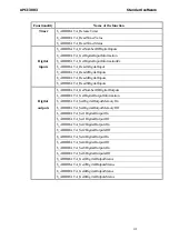
Standard software 

Software functions  39 
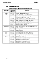
Software samples  42 

T


Technical data  11 
Test the board registration  23 

U


Update  24 
Use 

Intended use  7 
Usage restrictions  7 

User 

Personal protection  9 
Qualification  9 

V


virtual board  18 


 47 

Summary of Contents for APCI-3003

Page 1: ...DIN EN ISO 9001 2000 certified ADDI DATA GmbH Dieselstraße 3 D 77833 OTTERSWEIER 49 0 7223 9493 0 Technical description APCI 3003 Analog input board optically isolated Edition 01 09 11 2007 ...

Page 2: ...nly is protected by copyright Duplication of the information contained in the operating instructions and of any other product information or disclosure of this information for use by third parties is not permitted unless this right has been granted by the product licence issued Non compliance with this could lead to civil and criminal proceedings ADDI DATA software product licence Please read this...

Page 3: ...cautions yellow leaflet If this leaflet is not with the documentation please contact us and ask for it Observe the instructions of the manual Make sure that you do not forget or skip any step We are not liable for damages resulting from a wrong use of the board Used symbols i IMPORTANT designates hints and other useful information WARNING It designates a possibly dangerous situation If the instruc...

Page 4: ... Digital inputs 14 4 4 3 Digital outputs 14 4 4 4 Timer interruptible 16 bit 14 4 5 Component scheme 15 5 INSTALLATION OF THE BOARD 16 5 1 Opening the PC 16 5 2 Selecting a free slot 16 5 3 Plugging the board into the slot 17 5 4 Closing the PC 17 6 SOFTWARE 18 6 1 Board registration 19 6 1 1 Installation of a new board 19 ADDevice Manager 20 6 1 2 Changing the registration of a board 21 Descripti...

Page 5: ...1 8 1 Block diagram 31 8 2 Analog inputs 31 8 2 1 Overview 31 8 2 2 Voltage ranges 31 8 2 3 Analog input switch 32 8 2 4 Input modes of the analog inputs 32 1 Simple mode 32 2 Scan modes 33 3 Sequence modes 36 4 Auto refresh mode 38 9 STANDARD SOFTWARE 39 9 1 Software functions 39 9 2 Software samples 42 10 APPENDIX 43 10 1 Glossary 43 10 2 Index 46 5 ...

Page 6: ...or analog inputs 25 Fig 7 2 Analog input at the PX 901 AG 25 Fig 7 3 16 pin connector on a 15 pin SUB D female connector 26 Fig 7 4 Digital inputs and outputs at the PX 901 ZG 26 Fig 7 5 Connection principle of the analog inputs 28 Fig 7 6 Connection of the digital inputs 28 Fig 7 7 Connection of the digital outputs 29 Fig 7 8 Connection of the APCI 3003 to the screw terminal panels30 Fig 8 1 Bloc...

Page 7: ...osive atmospheres The APCI 3003 board must not be used as electrical equipment according to the Low Voltage Directive 2006 95 EC 1 3 General description of the board Data exchange between the APCI 3003 board and the peripheral is to occur through a shielded cable This cable must be connected to the 15 pin SUB D connector of the APCI 3003 board The board has 4 input channels for processing analog s...

Page 8: ...r to putting the device into operation The use of the board according to its intended purpose includes observing all advices given in the Technical description and in the Safety leaflet Uses beyond these specifications are not allowed The manufacturer is not liable for any damages which would result from the non observance of this clause Make sure that the board remains in its protective packing u...

Page 9: ... in electronics are entitled to perform the following works installation use maintanance 2 2 Personal protection Consider the country specific regulations about the prevention of accidents electrical and mechanical installations radio interference suppression 9 ...

Page 10: ...Handling of the board APCI 3003 3 HANDLING OF THE BOARD Fig 3 1 Correct handling 10 ...

Page 11: ... available on request 4 2 Physical set up of the board The board is assembled on a 4 layer printed circuit card Dimensions 175 mm 99 mm Weight approx 160 g Installation in 32 64 bit PCI slot 5 V or 3 3 V Connection to the peripheral 37 pin SUB D male connector Accessories1 Cables For the analog inputs Standard round cable ST3003 A For the digital I O Standard round cable ST3003 D Screw terminal pa...

Page 12: ...emperature 0 to 60 C Storage temperature 25 to 70 C Relative humidity at indoor installation 50 at 40 C 80 at 31 C Minimum PC requirements PCI BIOS from Version 1 0 Bus speed 33 MHz Operating system Windows 2000 XP Linux other operating systems on request Slot PCI 5 V or PCI 3 3 V 32 bit Current consumption without load typic See table 10 APCI 3003 5 V from PC 1 55 A 4 4 1 Analog inputs Number of ...

Page 13: ... with lowpass filter first level Input impedance 1012 Ω 5 nF Digital codification linear Analog Input Binary Code HEX Code Bipolar Unipolar 10V 0V 0000000000000000 0000 0V 5 V 1000000000000000 8000 10 V 10 V 1111111111111111 FFFF Optical isolation from the PC 1000 V Temperature drift 10 ppm K Linearity error of the ADC 1 22 mV typ 2 44 mV max Calibration of the inputs Bipolar offset calibration va...

Page 14: ...ne second tested Logic 0 level 0 14 V Logic 1 level 19 30 V Frequency 1 MHz 4 4 3 Digital outputs Number 4 Type Open Collector OC Max switch current 50 mA typ Voltage range 5 30 V Optical isolation from the PC 1000 V DC one second tested Switching time load 50 mA Switch on 2 µs Switch off 36 µs 4 4 4 Timer interruptible 16 bit Number 1 Time base us ms s 14 ...

Page 15: ...APCI 3003 Technical data 4 5 Component scheme Fig 4 1 Component scheme 15 ...

Page 16: ...he socket Open your PC as described in the manual of the PC manufacturer 5 2 Selecting a free slot Plug the board into a free PCI 5 V or PCI 3 3 V 32 64 bit slot Fig 5 1 Types of slots Remove the back cover of the selected slot according to the instructions of the PC manufacturer Keep the back cover You will need it if you remove the board Discharge yourself from electrostatic charges Take the boa...

Page 17: ...to the chosen slot Fig 5 2 Inserting the board Fasten the board to the rear of the PC housing with the screw which was fixed on the back cover Fig 5 3 Fastening the board at the back cover Tighten all the loosen screws 5 4 Closing the PC Close your PC as described in the manual of the PC manufacturer 17 ...

Page 18: ...and Windows XP 2000 98 The user can register all hardware information necessary to operate the ADDI DATA PC boards ADDIDRIVER contains API functions to operate the universal ADDI DATA boards in 32 bits ADDevice Manager configures the resources of the ADDI DATA virtual board see below ADDI DATA virtual board ADDI DATA software is based on the principle of a virtual board It transposes the different...

Page 19: ...w board is recognised the following window is displayed Fig 6 1 New inserted board example The boards which have been removed from the PC since the last ADDIREG start are listed in the upper table The new inserted boards are listed in the lower table In case further information is required for the operation of the board click on More Information ADDevice Manager is started 19 ...

Page 20: ...ard V software and the real board R board The following parameters are listed Module number Number of resources Index The first index line represents the number of the first resource left virtual resource right real board The second index line represents the number of the last resource left virtual resource right real board Type 24 V 5 V voltage current HS OC High Side Open collector etc If in thi...

Page 21: ... the registration you can close the window of ADDevice Manager The board is ready to operate 6 1 2 Changing the registration of a board At any time you can change the current board configuration of the APCI 3003 with ADDIREG Description of the ADDIREG program The program is automatically installed with ADDIPACK Start ADDIREG under Start Programs ADDIPACK ADDIREG i IMPORTANT First quit all the appl...

Page 22: ... the board uses no DMA or if the board is no ISA board More information Additional information like the identifier string or the installed COM interfaces If the board is programmed with ADDIDRIVER this information also is displayed Text boxes Base address name Description of the used base addresses for the board You can select a name through the pull down menu The corresponding address range is di...

Page 23: ...on Controls if there is a conflict between the board and other devices installed in the PC A message indicates the parameter which has generated the conflict If no conflict has occurred Test of device registration OK is displayed Deinstall registration Deinstalls the registrations of all boards listed in the table and deletes the entries of the boards in the Windows Registry Print registration Pri...

Page 24: ...ownloads of standard software You can download the latest version of the software for the board APCI 3003 from the internet http www addi data com i IMPORTANT Before using the board or in case of malfunction during operation check if there is an update of the product technical description driver The current version can be found on the internet or contact us directly 24 ...

Page 25: ...APCI 3003 Connecting the peripheral 7 CONNECTING THE PERIPHERAL 7 1 Connector pin assignment Fig 7 1 15 pin SUB D male connector analog inputs Fig 7 2 Analog input at the PX 901 AG 25 ...

Page 26: ...Connecting the peripheral APCI 3003 Fig 7 3 16 pin connector on a 15 pin SUB D female connector Fig 7 4 Digital inputs and outputs at the PX 901 ZG 26 ...

Page 27: ... analog inputs 37 pin SUB D connector Pin 1 20 2 21 3 22 4 23 5 24 6 25 7 26 8 27 8 9 1 10 2 11 3 12 4 13 5 14 6 15 7 Table 7 2 ST3003 D Digital inputs and outputs at the PX 901 ZG 15 pin SUB D connector 37 pin SUB D connector Pin 1 20 2 21 3 22 4 23 5 24 6 25 7 26 8 27 9 1 10 2 11 3 12 4 13 8 14 7 15 5 6 27 ...

Page 28: ...Connecting the peripheral APCI 3003 7 1 1 Analog inputs Fig 7 5 Connection principle of the analog inputs 7 1 2 Digital inputs and outputs Fig 7 6 Connection of the digital inputs 28 ...

Page 29: ...APCI 3003 Connecting the peripheral Fig 7 7 Connection of the digital outputs 29 ...

Page 30: ...Connecting the peripheral APCI 3003 7 2 Connection to the screw terminal panels Fig 7 8 Connection of the APCI 3003 to the screw terminal panels 30 ...

Page 31: ...converter All 4 analog modules are always started synchronously only the parameterized channels will be written fort he user into an especially designed read register FIFO AUTOREFRESHRAM The analog acquisition also can be triggerd through a digital input see chapter 8 2 4 input modes 8 2 2 Voltage ranges The analog input ranges 0 10V 10V 0 5V 5V 0 2V 2V 0 1V 1V 0 20 mA and the gain can be configur...

Page 32: ...al assembly for the version current C DF optional assembly for DF filter Limit frequency fg 1 212 2 KHz 2 п 75 Ω 75 Ω CDF C1 C2 C DF no components inserted 8 2 4 Input modes of the analog inputs On the board are 4 differential channels available for the analog inputs The acquisition can be realized in the following modes 1 Simple mode 2 Scan mode 3 Sequence mode 4 Auto refresh mode 1 Simple mode T...

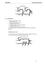
Page 33: ...are scan d Continuous software scan with timer delay e Continuous hardware scan f Continuous hardware scan with timer delay The following section will describe the above mentioned scan modes more detailed a Single software scan The user interrupt routine is called after the last IRQ ADDI DATA driver Note In the scan mode no DMA functionality is used 33 ...

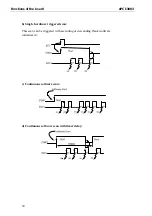
Page 34: ... the board APCI 3003 b Single hardware triggered scan This scan can be triggered with ascending or descending flank software initializes it c Continuous software scan d Continuous software scan with timer delay 34 ...

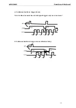
Page 35: ...APCI 3003 Functions of the board e Continuous hardware triggered scan Note In this scan mode the external signal triggers only one scan at once f Continuous hardware triggered scan with timer delay 35 ...

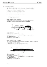
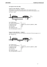
Page 36: ...ce after 5 acquisitions and the acquisition is stopped after 3 sequences dw_NbrOfChannel 5 dw_SequenceChannelArray 0 1 2 3 4 b_DelayTimeMode ADDIDATAG_DELAY_NOT_USED dw_SequenceCounter 3 dw_InterruptSequenceCounter 1 Simple sequence mode example 2 Here the interrupt occurs after 2 sequences 10 acquisitions and the acquisition is stopped via the following function b_ADDIDATA_StopAnalogInputSequence...

Page 37: ..._SequenceChannelArray 0 1 2 3 4 b_DelayTimeMode ADDIDATAG_DELAY_MODE1_USED b_DelayTimeUnit 1 µs dw_DelayTime 100 dw_SequenceCounter 2 dw_InterruptSequenceCounter 2 Sequence mode with delay example 2 The delay time after the end of one sequence to the start of the next sequence ist in this example 20 µs dw_NbrOfChannel 5 dw_SequenceChannelArray 0 1 2 3 4 b_DelayTimeMode ADDIDATAG_DELAY_MODE2_USED b...

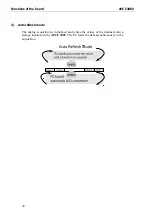
Page 38: ...the board APCI 3003 4 Auto refresh mode The analog acquisition is initialized and writes the values of the channels into a storage location on the APCI 3003 The PC reads the data asynchronously to the acquisition 38 ...

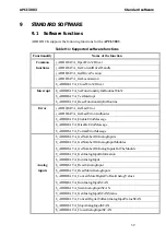
Page 39: ...ne Error i_ADDIDATA_GetLastError i_ADDIDATA_GetLastErrorAndSource b_ADDIDATA_EnableErrorMessage b_ADDIDATA_DisableErrorMessage b_ADDIDATA_FormatErrorMessage b_ADDIDATA_GetNumberOfAnalogInputs b_ADDIDATA_GetNumberOfAnalogInputModules b_ADDIDATA_GetNumberOfAnalogInputsForTheModule b_ADDIDATA_GetAnalogInputInformation b_ADDIDATA_InitAnalogInput Analog b_ADDIDATA_Read1AnalogInput inputs b_ADDIDATA_Rea...

Page 40: ...ATA_ConvertAnalogInputSequenceDigitalToRealAnalogValue b_ADDIDATA_StopAnalogInputSequenceAcquisition b_ADDIDATA_GetAnalogInputSequenceAcquisitionHandleStatus b_ADDIDATA_ReleaseAnalogInputSequenceAcquisition b_ADDIDATA_GetAnalogInputHardwareTriggerInformations b_ADDIDATA_EnableDisableAnalogInputHardwareTrigger b_ADDIDATA_GetAnalogInputHardwareTriggerStatus b_ADDIDATA_EnableDisableAnalogInputSoftwar...

Page 41: ...8DigitalInputs b_ADDIDATA_GetNumberOfDigitalOutputs b_ADDIDATA_GetDigitalOutputInformation Digital b_ADDIDATA_SetDigitalOutputMemoryOn outputs b_ADDIDATA_SetDigitalOutputMemoryOff b_ADDIDATA_Set1DigitalOutputOn b_ADDIDATA_Set1DigitalOutputOff b_ADDIDATA_Set2DigitalOutputsOn b_ADDIDATA_Set2DigitalOutputsOff b_ADDIDATA_Set4DigitalOutputOn b_ADDIDATA_Set4DigitalOutputOff b_ADDIDATA_Set8DigitalOutputs...

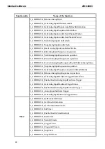
Page 42: ...upt SAMPLE06 Tests the Auto Refresh sequence acquisition SAMPLE 07 Initializes SCAN with interrupt Digital inputs SAMPLE00 Receives the information of the selected digital input channel SAMPLE01 Reads 1 digital input SAMPLE02 Reads 2 digital inputs SAMPLE03 Reads 4 digital inputs Digital SAMPLE01 Tests 1 digital output with without output buffer outputs SAMPLE02 Tests 2 digital outputs with withou...

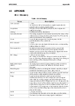
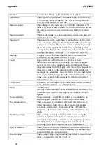
Page 43: ... respecting the time It will always fluctuate slightly Especially at switching on and switching off the transition behaviour is of high significance Differential inputs DIFF An analog input with two input terminals neither of which is grounded whose value is the difference between the two terminals Disturb signal Interferences that occur during the transfer caused by reduced bandwidth attenuation ...

Page 44: ...finite the H level is the digital 1 L represents the range that is closer to Minus infinite the L level is the digital 0 The rising edge is the transition from the 0 state to the 1 state and the falling edge is the transition from the 1 state to the 0 state Limit value Exceeding the limit values even for just a short time can lead to the destruction or to a loss of functionality MUX Multiplexer An...

Page 45: ...lution can resolve 1 part in 4096 Scan mode Scan modes are Single software scan single hardware triggered scan continuous software scan continuous software scan with timer delay continuous hardware triggered scan and continuous hardware triggered scan with timer delay Sensor A device that responds to physical stimuli heat light sound pressure motion etc and produces a corresponding electrical outp...

Page 46: ...rts an operation Digital trigger An event that occurs at a user selected point on a digital input signal The polarity and sensitivity of the digital trigger can often be programmed TTL transistor transistor logic A popular logic circuit family that uses multiple emitter transistors 10 2 Index A Accessories 11 ADDevice Manager 18 20 ADDEVICE MAPPE 18 ADDIDRIVER 18 ADDIPACK 18 ADDIREG 18 Buttons 23 ...

Page 47: ...ements 12 Physical set up of the board 11 S Scan mode Continuous hardware triggered scan 35 Continuous hardware triggered scan with timer delay 35 Continuous software scan 34 Continuous software scan with timer delay 34 Single hardware triggered scan 34 Single software scan 33 Sequence mode Simple 36 With delay 37 Software 18 Standard software Software functions 39 Software samples 42 T Technical ...

Reviews: