background image

66              ICX-250 Diagnostics

LED Indicators

ADCP-62-023

Issue 1, September 1998

© 1998, ADC Telecommunications, Inc.

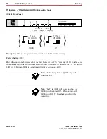
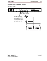
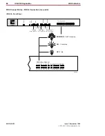
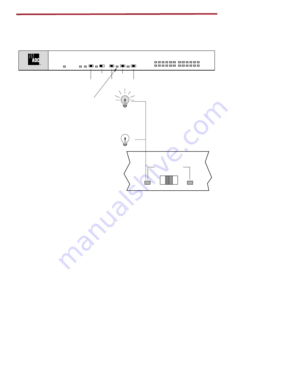
Data Port 1 - Test Pattern Sync 

(Green LED)

ICX-250 - Front Panel

ICX-250

1 3 5 7 9 11 13 15 17 19 21 23

2 4 6 8 10 12 14 16 18 20 22 24

FXS Status Channel

Data Loop 2

Lcl. / Off / Net.

Data Loop 1

Lcl. / Off / Net.

T1 Loop

Net. / Off / Lcl.

1 / Off / 2

Off / QRSS

T1 Status

T1 Loop

Test Pattern

Test Pattern

T1 T

est

Self Check

11287-A

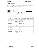
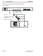
ON:  Sync

A Green LED indicates that the 
test pattern received by the 
Data Port (1 or 2) pattern 
detector matches the pattern 
generated by the system.

OFF:  No Sync

Test Pattern

1   Off   2

Summary of Contents for ICX-250

Page 1: ...ADCP 62 023 Issue 1 September 1998 1027494 ICX 250 User Manual ...

Page 2: ...n no event shall ADC be liable for any damages resulting from loss of data loss of use or loss of profits and ADC further disclaims anyand all liability for indirect incidental special consequential or other similar damages This disclaimer of liability applies to all products publications and services during and after the warranty period This publication may be verified at any time by contacting A...

Page 3: ...INSTALLING THE ICX 250 8 CHOOSING A SITE FOR THE ICX 250 8 RACK MOUNTING 9 LOCATING THE ICX 250 ON A DESKTOP 11 WALL MOUNTING 12 THE ICX 250 UNIT 13 INTERNAL LAYOUT 14 INTERNAL DIP SWITCHES 18 DIP SWITCH SETTINGS 18 SETUP AND CONFIGURE THE ICX 250 20 SWITCHES 20 FXS SUPERVISION TABLE 25 EXTERNAL DIP SWITCHES 31 DIP SWITCH SETTINGS 31 CONFIGURATION REFERENCE DATA 41 CONNECTOR TYPE 44 CONNECTOR PINO...

Page 4: ...8 1998 ADC Telecommunications Inc TABLE OF CONTENTS Content Page WARRANTY SOFTWARE 69 REPAIR ADVANCE REPLACEMENT POLICY 69 REPAIR CHARGES 69 REPLACEMENT SPARE PRODUCTS 70 RETURNED MATERIAL 70 SYSTEM INTEGRATION SERVICES 71 CUSTOMER SUPPORT SERVICES 71 ...

Page 5: ...ssary consult with the appropriate regulatory agencies and inspection authorities to ensure compliance 8 A rare phenomenon can create a voltage potential between the earth grounds of two or more buildings If products installed in separate buildings are interconnected the voltage potential may cause a hazardous condition Consult a qualified electrical consultant to determine whether or not this phe...

Page 6: ...d and used in accordance with this User Manual may cause harmful interference to radio communications Operation of this equipment in a resi dential area may cause harmful interference If this happens the user would be required to correct the interference at his own expense FCC REGULATORY REQUIREMENTS Notice to Users of T1 Service The following instructions are provided to ensure compliance with th...

Page 7: ...omplaint with the FCC 6 An affidavit must be completed by the installer 7 In the event of equipment malfunction all repairs should be performed by our Company or an authorized agent It is the responsibility of users requiring service to report the need for service to our Company or to one of our authorized agents UL APPROVED The ICX 250 has been designed and tested in accordance with the requireme...

Page 8: ... Issue 1 September 1998 ADCP 62 023 1998 ADC Telecommunications Inc C H A P T E R 1 Welcome This chapter introduces you to the features and benefits of ICX 250 Contents Unpacking the ICX 250 2 Product Overview 3 ...

Page 9: ... power plug A 2 Conductor alarm closure plug 6 6 x 5 16 self tapping screws 4 12 24 x 1 2 screws 1 AC power cord ICX 250 User Manual this book The ICX 250 U ser M anual contains common tasks configuration installation maintenance and testing of the unit Hardware and Cabling The ICX 250 unit comes packaged with an AC power cord to provide power to the unit It is also shipped with two angle brackets...

Page 10: ... bundled service arrangements For sites needing up to 24 analog lines with or without data requirements ADC s ICX 250 is an ideal solution The ICX 250 s primary function is to allow for remote termination of lines from a centrally located switch Data ports are also provided on the unit for those applications where high speed data deployment would be required The ICX 250 product is complimentary to...

Page 11: ... made possible by the exchange of messages between the Local Digital Switch LDS and remote terminal RT Although commonly referred to as the TR 08 standard the RT channel numbering scheme supported by the ICX 250 unit is described in section 9 9 of the Bellcore publication TR TSY 000057 The ICX 250 provides SLC 96 Frame Format and Data Link When a T1 port is configured for TR 08 format the voice ch...

Page 12: ... Frame Format Line Code CSU Line Build Out LBO DSX Line Length Clocking FDL One RJ48 D4 ESF TR 08 AMI B8ZS 0 dB 7 5 dB 15 0 dB 0 6 dB at 0 266 ft 1 8 dB at 266 533 ft 3 0 dB at 533 655 ft Internal Stratum 4 Line Per ANSI T1 403 and AT T TR62411 FXS Interface Physical FXS Supervision Mode FXS Signaling TLP Impedance Ringing Voltage One 50 pin Female Amphenol FXS FXS DN FXS DN Wink TR 08 Loop Start ...

Page 13: ...1998 ADC Telecommunications Inc C H A P T E R 2 System Basics This chapter gives you quick simple instructions to get you up and running You will also learn how to install and mount the ICX 250 unit Contents Installing the ICX 250 8 The ICX 250 Unit 13 ...

Page 14: ...s equipped with a fan to ensure proper cooling and reliability In the event that the installation environment temperature exceeds the standards above it is recommended that adjustments be made Improper operation outside of these temperatures may result in performance degradation Precautionary Procedures There are several precautions to take before installing and or servicing the ICX 250 unit CAUTI...

Page 15: ...ble routing Provide at least 2 inches of clearance between each ICX 250 unit to allow for removal of the top if necessary for resetting of switches 1RWH Check all grounding instructions when installing the ICX 250 unit in a rack Proper grounding is mandatory at all times The following figure depicts a 19 rack mount configuration FXS Channel Status Data Loop 2 Lcl Off Net 1 3 5 7 9 11 13 15 17 19 2...

Page 16: ...DCP 62 023 Issue 1 September 1998 1998 ADC Telecommunications Inc The following figure depicts a 23 rack mount configuration ATTENTION Set all options prior to installing mounting brackets top cover cannot be removed once brackets are in place ...

Page 17: ...e unit when mounted on a flat surface Removing them may damage the unit ICX 250 1 3 5 7 9 11 13 15 17 19 21 23 2 4 6 8 10 12 14 16 18 20 22 24 FXS Status Channel T1 Status T1 Loop Test Pattern Test Pattern T1 Test Self Check ICX 250 1 3 5 7 9 11 13 15 17 19 21 23 2 4 6 8 10 12 14 16 18 20 22 24 FXS Status Channel T1 Status T1 Loop Test Pattern Test Pattern T1 Test Self Check ICX 250 1 3 5 7 9 11 1...

Page 18: ...cess to switches When attaching unit s to a wall make sure that appropriate fasteners such as masonry anchors heavy duty wood screws or expansion bolts are used for heavy objects ATTENTION Set all options prior to installing mounting brackets top cover cannot be removed once brackets are in place Note Additional support hardware may be necessary not included with unit to secure the unit properly t...

Page 19: ... 21 23 2 4 6 8 10 12 14 16 18 20 22 24 FXS Status Channel Data Loop 2 Lcl Off Net Data Loop 1 Lcl Off Net T1 Loop Net Off Lcl 1 Off 2 Off QRSS T1 Status T1 Loop Test Pattern Test Pattern T1 Test Self Check 11261 A 120 VAC 6A 60Hz 24 48 VDC G T1 Rx Tx T1 Line T1 Data 2 Data 2 Data 1 1 12 13 24 Alm Data 1 FXS Loopback FXS Loop Pairs 11264 A 25 PAIR AMPHENOL CONNECTOR FOR 24 FXS TIP AND RING PAIRS DI...

Page 20: ...s Inc Internal Layout 12 FXS Analog Voice Ports The illustration below shows the internal layout of the 12 FXS analog voice port unit 1 2 3 4 5 6 7 8 ON DIP S7 1 2 3 4 5 6 7 8 ON DIP S6 1 2 3 4 5 6 7 8 ON DIP S14 1 2 3 4 5 6 7 8 ON DIP S16 1 2 3 4 5 6 7 8 ON DIP S15 S1 S2 S3 S4 S5 FRONT BACK FAN ...

Page 21: ... illustration below shows the internal layout of the 24 FXS analog voice port unit 1 2 3 4 5 6 7 8 ON DIP S7 1 2 3 4 5 6 7 8 ON DIP S6 1 2 3 4 5 6 7 8 ON DIP S17 1 2 3 4 5 6 7 8 ON DIP S18 1 2 3 4 5 6 7 8 ON DIP S19 1 2 3 4 5 6 7 8 ON DIP S14 1 2 3 4 5 6 7 8 ON DIP S16 1 2 3 4 5 6 7 8 ON DIP S15 S1 S2 S3 S4 S5 FRONT BACK FAN ...

Page 22: ...nc C H A P T E R 3 Configuring the ICX 250 Inside this chapter you will learn how to configure the ICX 250 unit using internal and external switch settings Contents Internal DIP Switches 18 Setup and Configure the ICX 250 20 Switches 20 External DIP Switches 31 Configuration Reference Data 41 ...

Page 23: ...and three on the auxiliary board Note The individual switches on each switch assembly operate independently of one another DIP Switch Settings Locate the DIP switch internally that describes the function you wish to effect The top cover of the unit displays the configurable options Use the tip of a small object to change the switch settings The switches will glide easily into place CAUTION Access ...

Page 24: ... Telecommunications Inc 1 2 3 4 5 6 7 8 ON DIP S7 1 2 3 4 5 6 7 8 ON DIP S6 1 2 3 4 5 6 7 8 ON DIP S17 1 2 3 4 5 6 7 8 ON DIP S18 1 2 3 4 5 6 7 8 ON DIP S19 1 2 3 4 5 6 7 8 ON DIP S14 1 2 3 4 5 6 7 8 ON DIP S16 1 2 3 4 5 6 7 8 ON DIP S15 S1 S2 S3 S4 S5 BACK FRONT S16 S15 S19 S18 S17 S14 S7 S6 ...

Page 25: ...Sub scriber FXS DN Foreign Exchange Subscriber Defined Network FXS DN WINK Foreign Exchange Subscriber Defined Network Wink Start Operation TR 08 Frame Format Signaling and Data Link as outlined in TR TSY 000008 Mode 1 for circuits using AT T Subscriber Loop Carriers SLC 96 facilities FXS Supervision Type for entire bank of 12 lines see page 24 S6 S7 positions 3 4 and 5 Internal Loop Start Single ...

Page 26: ...condition in the T1 con nection between the ICX 250 and the network the FXS Ports will be put into the Idle state immediately for 3 seconds and then put in the Busy state and remain in this condi tion until the T1 has been restored FXS Ringback Tone see page 29 S6 S7 position 7 Internal On Off On Ringback tones will be sent on the corresponding DS0 s for the duration of ringing on the line Off Rin...

Page 27: ... see page 34 S1 positions 6 and 7 Back 0 dB 7 5 dB 15 0 dB Selects one of three line build out options for short 15 0 dB medium 7 5 dB and long 0 dB loops DATA PORTS Data Ports 1 and 2 Number of Timeslots see page 35 S2 dataport 2 positions 1 2 3 4 and 5 S3 dataport 1 positions 1 2 3 4 and 5 Back 0 1 2 3 24 Selects the number of timeslots that data from Data Port 1 and or 2 will be mapped onto Dat...

Page 28: ...ptions are FXS FXS DN FXS DN WINK and TR 08 Factory Setting FXS FXS Foreign Exchange Subscriber FXS DN Foreign Exchange Subscriber Defined Network FXS DN WINK Foreign Exchange Subscriber Defined Network Wink Start Operation TR 08 Signaling as outlined in TR TSY 000008 Mode 1 for circuits using AT T Subscriber Loop Carriers SLC 96 facilities 1 2 3 4 5 6 7 8 ON DIP S7 1 2 3 4 5 6 7 8 ON DIP S6 1 2 3...

Page 29: ...des disconnect when FXS is connected to voice messaging system Ground Start Used with two way PBX lines Ground Start Automatic Used with equipment requiring fast response time to the central office CO Ground Start Immediate Used with equipment requiring fast response time to the station or PBX Single Party Single Part Service for SLC 96 Universal Voice Grade Toll quality voice for SLC 96 Universal...

Page 30: ...eans any active calls in that FXS line group will be dropped FXS Supervision Table Legend e g S1 position 5 01001 means Mode FXS DN Type LS fd LS Loop Start LS fd Loop Start Forward Disconnect GS Ground Start GSa Ground Start Automatic GSi Ground Start Immediate SP Single Party UVG Universal Voice Grade UVGa Universal Voice Grade Automatic Mode 1 2 3 4 5 Type 000 001 100 101 110 FXS 00 LS LS fd GS...

Page 31: ...would be set to the On setting Receive side settings would be changed from 9 dB to 3 dB by moving the related switch position to Off See the chart on page 27 for more detail on the switch settings 3dB Transmit Receive path will be attenuated by 3 dB 0 5 9dB Transmit Receive path will be attenuated by 9 dB 0 5 ATTENTION The above FXS Port settings are repeated for each of the 12 or 24 lines 1 2 3 4...

Page 32: ... OFF 5 OFF 6 ON 5 ON 3 4 OFF 3 OFF 4 ON 3 ON 4 2 OFF 1 OFF 2 ON 1 ON 5 S15 8 OFF 7 OFF 8 ON 7 ON 6 6 OFF 5 OFF 6 ON 5 ON 7 4 OFF 3 OFF 4 ON 3 ON 8 2 OFF 1 OFF 2 ON 1 ON 9 S16 8 OFF 7 OFF 8 ON 7 ON 10 6 OFF 5 OFF 6 ON 5 ON 11 4 OFF 3 OFF 4 ON 3 ON 12 2 OFF 1 OFF 2 ON 1 ON 13 S17 8 OFF 7 OFF 8 ON 7 ON 14 6 OFF 5 OFF 6 ON 5 ON 15 4 OFF 3 OFF 4 ON 3 ON 16 2 OFF 1 OFF 2 ON 1 ON 17 S18 8 OFF 7 OFF 8 ON ...

Page 33: ...elay In the event of an alarm condition in the T1 connection between the ICX 250 and the network the FXS Ports will be put into the Idle state immediately for 3 seconds and then put into the Busy state and remain in this condition until the T1 has been restored The DIP switch settings shown in the illustration above are for Switch S6 and S7 1 2 3 4 5 6 7 8 ON DIP S7 1 2 3 4 5 6 7 8 ON DIP S6 1 2 3...

Page 34: ...channels by the unit if not provided by the Switch or PBX for the duration of ringing on the line OFF Ringback provided by PBX or Switch The DIP switch settings shown in the illustration above are for Switches S6 and S7 1 2 3 4 5 6 7 8 ON DIP S7 1 2 3 4 5 6 7 8 ON DIP S6 1 2 3 4 5 6 7 8 ON DIP S17 1 2 3 4 5 6 7 8 ON DIP S18 1 2 3 4 5 6 7 8 ON DIP S19 1 2 3 4 5 6 7 8 ON DIP S14 1 2 3 4 5 6 7 8 ON D...

Page 35: ...nly on switch 7 and is applicable only on the 12 port model Depending on the services provided by your carrier for voice and data you may need to reassign the FXS timeslots of the 12 FXS port model Timeslots 13 to 24 will be assigned in order to allocate data to the lower timeslots The DIP switch setting shown in the illustration above is for Switch S7 ONLY 1 2 3 4 5 6 7 8 ON DIP S7 1 2 3 4 5 6 7 ...

Page 36: ...utlines the location of these DIP switches Note The individual switches on each switch assembly operate independently of one another ICX 250 Rear Panel Switch numbers S1 through S5 are shown on the board within the unit DIP Switch Settings Locate the DIP switch on the rear panel that describes the function you wish to effect Use the tip of a small object to change the switch settings The switches ...

Page 37: ... slips on the T1 T1 Interface Line Code DIP switch back ICX 250 Rear Panel Switch numbers S1 through S5 are shown on the board within the unit Description S1 position 3 is used to select the T1 line code Factory Setting B8ZS Line Code Selects the line code on the T1 interface Selections AMI B8ZS 120 VAC 6A 60Hz 24 48 VDC G T1 Rx Tx T1 Line T1 Data 2 Data 2 Data 1 1 12 13 24 ON DIP 1 2 3 4 5 6 7 Al...

Page 38: ...r the T1 interface will be recovered from the line receive signal Internal Clock for the T1 interface will be taken from an on board 1 544 MHz clock meeting the Stratum 4 requirements Note Failure of external clock causes unit to switch to internal clock When external clock is restored the unit will switch back to external clock source 120 VAC 6A 60Hz 24 48 VDC G T1 Rx Tx T1 Line T1 Data 2 Data 2 ...

Page 39: ...ough S5 are shown on the board within the unit Description S1 position 6 and 7 are used to select CSU DSX line build out or line length Factory Setting CSU 0dB Line Build Out Selects one of three line build out and line length options for either CSU or DSX interfaces Selections CSU 0 dB 7 5 dB and 15 0 dB DSX 0 6 dB at 250 ft 1 8 dB at 500 ft 3 0 dB at 700 ft 120 VAC 6A 60Hz 24 48 VDC G T1 Rx Tx T...

Page 40: ...idth Factory Setting All switches are set to zero data ports inactive Number of Timeslots Selects the number of consecutive timeslots that data from Data Port 1 and or 2 will be mapped onto Please refer to Decimal Binary Conversion Table see page 36 for Data Port Configuration to aid in selecting N Drawing above indicates switch settings if timeslot N 13 Selected quantity of timeslots x 64K Data P...

Page 41: ...andwidth Timeslot Switch Setting 0 00000 832K 13 01101 64K 1 00001 896K 14 01110 128K 2 00010 960K 15 01111 192K 3 00011 1024K 16 10000 256K 4 00100 1088K 17 10001 320K 5 00101 1152K 18 10010 384K 6 00110 1216K 19 10011 448K 7 00111 1280K 20 10100 512K 8 01000 1344K 21 10101 576K 9 01001 1408K 22 10110 640K 10 01010 1472K 23 10111 704K 11 01011 1536K 24 11000 768K 12 01100 Starting T S 6 7 8 9 1 o...

Page 42: ...arting timeslot 1 3 5 7 9 etc for data port 1 Factory Setting All switches are set to zero data ports not active Starting Timeslot Selects first T1 timeslot that data from Data Port 1 and or 2 will be mapped 1 3 5 7 9 23 Please refer to Decimal Binary Conversion Table see page 36 to aid in selecting the startingtimeslot Drawingabove indicates switch settings using timeslot 6 asthe starting timeslo...

Page 43: ...0 Rear Panel Switch numbers S1 through S5 are shown on the board within the unit Description S2 and S3 position 11 selects the data interface for Data Ports 2 and 1 Factory Setting V 35 EIA530A Data Ports 1 or 2 use the EIA530A standard V 35 Data Ports 1 or 2 use the V 35 standard 120 VAC 6A 60Hz 24 48 VDC G T1 Rx Tx T1 Line T1 Data 2 Data 2 Data 1 1 12 13 24 ON DIP 1 0 1 2 3 4 5 6 7 8 9 10 11 12 ...

Page 44: ...d or Channel Unassigned DIP switch back ICX 250 Rear Panel Switch numbers S1 through S5 are shown on the board within the unit Description Used to set loopback for each FXS channel Factory Setting OFF ON Breaks the connections to and from the FXS Ports and loops the receive data back onto the transmit path towards the T1 In the case of unassigned channels provides an idle termination 120 VAC 6A 60...

Page 45: ... idle termination T1 Network ICX 250 Transmit Receive FXS 1 FXS 1 Loopback T24 Network ICX 250 Transmit Receive FXS 24 FXS 24 Loopback 11276 A The selected DS0 is looped after leaving the framer before reaching the FXS Interface The CPU is used to control this loopback via the Time Slot Assigner TSA a part of the CPU Subsystems T1 Line Interface Unit T1 Framer and CPU are exercised ...

Page 46: ... 6 7 8 1 2 3 4 5 6 7 8 1 2 3 4 5 6 7 8 Ports 16 15 14 13 Ports 16 15 14 13 Ports 24 23 22 21 Ports 24 23 22 21 Ports 20 19 18 17 Ports 20 19 18 17 FXS Transmission Level FXS Transmission Level Ports 13 24 Ports 1 12 View From Top Rear 0 1 2 3 4 5 6 7 8 9 10 11 12 00000 00001 00010 00011 00100 00101 00110 00111 01000 01001 01010 01011 01100 1 3 5 7 9 11 13 15 17 19 21 23 0000 0001 0010 0011 0100 01...

Page 47: ...ommunications Inc C H A P T E R 4 Electrical Installation When you are ready to go beyond the basics of the ICX 250 unit use this chapter to learn specifics on grounding cabling and the necessary power requirements for operation Contents Connector Type 44 Power Requirements 47 ...

Page 48: ...sition plug included with Kit of Parts A relay closure that sends alarms out to an external alarm system Data 1 and Data 2 DB25 Female Data Port 1 signals and Data Port 2 signals T1 Line RJ48 Transmit and Receive pairs T1 Dual Bantam Jack monitor jacks For bridged access onto the T1 transmit and receive pairs 24 48VDC G 1 8 9A Max 3 position plug included with Kit of Parts For DC power input Note ...

Page 49: ...e Line Signal Detector DCD CF A DCE X X 9 Receive Signal Element Timing RXCLK DD B DCE X X 10 Receive Line Signal Detector DCD CF B DCE X 11 Transmit Signal Element Timing DTE TXCLK DA B DTE X 12 Transmit Signal Element Timing DCE TXCLK DB B DCE X X 13 Clear to Send CTS CB B DCE X 14 Transmit Data TXD BA B DTE X X 15 Transmit Signal Element Timing DCE TXCLK DB A DCE X X 16 Receive Data RXD BB B DC...

Page 50: ...3 R 13 2 T 27 14 T 39 2 R 2 14 R 14 3 T 28 15 T 40 3 R 3 15 R 15 4 T 29 16 T 41 4 R 4 16 R 16 5 T 30 17 T 42 5 R 5 17 R 17 6 T 31 18 T 43 6 R 6 18 R 18 7 T 32 19 T 44 7 R 7 19 R 19 8 T 33 20 T 45 8 R 8 20 R 20 9 T 34 21 T 46 9 R 9 21 R 21 10 T 35 22 T 47 10 R 10 22 R 22 11 T 36 23 T 48 11 R 11 23 R 23 12 T 37 24 T 49 12 R 12 24 R 24 Not Assigned 50 Not Assigned 25 RJ 48 F Pin Signal 1 R1 2 T1 4 R ...

Page 51: ...le located on the back of the unit D C Power Installation When wiring to an external power source such as a battery rack fuse panel or circuit breaker make sure that the correct rating of wire is used It is recommended you use 20 to 18 gauge wire Note The ICX 250 unit can have both an AC and DC power source connected to it at the same time These two power inputs will share the power load However i...

Page 52: ...und lead to the ICX 250 chassis The ground lead must be connected to the chassis using a No 6 nut and lock washer combination The mounting location is labeled with the IEC 417 No 5019 symbol to identify this as the AC earth ground connection point This mounting stud is located next to the IEC 320 AC input connector The loop battery return and the FXS digital and analog circuitry must share a commo...

Page 53: ...mended for use with the ICX 250 unit Cable Used for Description Voice FXS Ports 50 pin Amphenol M to 50 pin Amphenol M 5 Data Data Ports EIA530A DB25M to DB25F Straight through 5 Data Data Ports V 35 DB25M to M34F Straight through 5 T1 RJ48 Port RJ48M to RJ48M Shielded 1 T1 RJ48 Port RJ48M to RJ48M Shielded 25 AC Power AC Power Input AC Power Cable 6 ...

Page 54: ...ember 1998 ADCP 62 023 1998 ADC Telecommunications Inc C H A P T E R 5 ICX 250 Diagnostics This chapter describes how to run test patterns and to diagnose events taking place within the ICX 250 unit Contents Testing 52 LED Indicators 61 ...

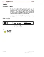
Page 55: ...Locate the slide switch on the front panel that implements the function desired Use the end of a small object or the tip of your finger to change the switch settings ICX 250 Front Panel ICX 250 1 3 5 7 9 11 13 15 17 19 21 23 2 4 6 8 10 12 14 16 18 20 22 24 FXS Status Channel Data Loop 2 Lcl Off Net Data Loop 1 Lcl Off Net T1 Loop Net Off Lcl 1 Off 2 Off QRSS T1 Status T1 Loop Test Pattern Test Pat...

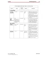
Page 56: ...S Ports and the T1 inter face are broken and a QRSS pattern is transmitted onto the T1 interface At this time the T1 Test Pattern LED will light when QRSS is being transmitted Note ONLY works with framed T1 DATA PORTS Loopback see page 58 Data Port 1 and 2 Loopback Front slide Local Network Off Local Breaks the receive signal on the network side between the Data Port 1 or 2 and the T1 interface an...

Page 57: ...e T1 transmit within the Framer chip Local Loops signal back to the network and breaks the transmit and receive paths between the LIU and the line and loops the T1 transmit signal onto the T1 receive within the LIU Note When operating the QRSS switch the T1 Loopback switch will be inoperative ICX 250 1 3 5 7 9 11 13 15 17 19 21 23 2 4 6 8 10 12 14 16 18 20 22 24 FXS Status Channel Data Loop 2 Lcl ...

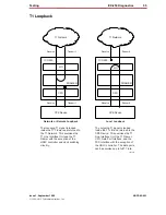
Page 58: ...cal Loopback The incoming T1 signal is looped inside the T1 Framer and returned to the T1 Network This exercises the T1 Line Interface Unit and the T1 Framer with the exception of the HDLC controller and clock switching circuitry The outgoing T1 signal is looped inside the T1 LIU and returned to the CPE Device This exercises the T1 Line Interface Unit the T1 Framer CPU Data Port Interface and the ...

Page 59: ... the T1 interface At this time the T1 Test pattern LED will light when QRSS is being transmitted see section on LED Note The T1 test pattern for QRSS only works with framed T1 Note The T1 test LED will come on when the QRSS switch is turned ON When operating the QRSS switch the T1 Loopback switch will be inoperative ICX 250 1 3 5 7 9 11 13 15 17 19 21 23 2 4 6 8 10 12 14 16 18 20 22 24 FXS Status ...

Page 60: ...ssue 1 September 1998 ADCP 62 023 1998 ADC Telecommunications Inc T1 Interface ICX 250 QRSS Transmitter 2047 2047 Pattern Detector Data Port 2 Data Port 1 Pattern Detector 2047 Transmitter 2047 Transmitter Internal Control and Routing ...

Page 61: ...r 2 transmit signal onto the receive side Network Breaks the transmit signal on the network side between the Data Port 1 or 2 and the T1 interface and loops the Data Port 1 or 2 receive signal onto the transmit side ICX 250 1 3 5 7 9 11 13 15 17 19 21 23 2 4 6 8 10 12 14 16 18 20 22 24 FXS Status Channel Data Loop 2 Lcl Off Net Data Loop 1 Lcl Off Net T1 Loop Net Off Lcl Data Loop 1 Lcl Off Net Da...

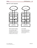
Page 62: ... used to control this loopback via the TSA Subsystems T1 Line Interface Unit T1 Framer and CPU are exercised The Data Port interface signal is looped inside the CPU and returned to the data port interface Sub systems CPU and Data Port inter face are exercised T1 Network ICX 250 Transmit Receive FRAMER LIU CPU CPE Device Data Port 1 and 2 11278 A T1 Network ICX 250 Transmit Receive Transmit Receive...

Page 63: ...nd injects the 2047 pattern onto the transmit path Test Data Port 2 Breaks the transmit and receive paths between Data Port 2 and the receiver and injects the 2047 pattern onto the transmit path Off 2047 function is disabled See diagram on page 55 ICX 250 1 3 5 7 9 11 13 15 17 19 21 23 2 4 6 8 10 12 14 16 18 20 22 24 FXS Status Channel Data Loop 2 Lcl Off Net Data Loop 1 Lcl Off Net T1 Loop Net Of...

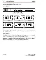
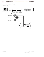
Page 64: ... page 63 RED Red Alarm YELLOW Yellow Alarm GREEN Normal T1 Loop Yellow LED see page 64 ON Network BLINKING Local OFF None T1 Test Pattern Sync Green LED see page 65 GREEN QRSS On OFF No QRSS Test Pattern Sync Green LED Data Port 1 see page 66 GREEN Sync OFF No Sync Test Pattern Sync Green LED Data Port 2 see page 67 GREEN Sync OFF No Sync FXS N Connection Green LED FXS Channel Status x 24 see page...

Page 65: ...X 250 1 3 5 7 9 11 13 15 17 19 21 23 2 4 6 8 10 12 14 16 18 20 22 24 FXS Status Channel Data Loop 2 Lcl Off Net Data Loop 1 Lcl Off Net T1 Loop Net Off Lcl 1 Off 2 Off QRSS T1 Status T1 Loop Test Pattern Test Pattern T1 Test Self Check 11283 A ICX 250 Self Check OFF Normal ON Failed Self Test during power up or a system failure occured during normal operation BLINKING Invalid Configuration ...

Page 66: ... 14 16 18 20 22 24 FXS Status Channel Data Loop 2 Lcl Off Net Data Loop 1 Lcl Off Net T1 Loop Net Off Lcl 1 Off 2 Off QRSS T1 Status T1 Loop Test Pattern Test Pattern T1 Test Self Check 11284 A OFF Red Alarm Indicates a loss of signal on the receive side of the T1 YELLOW Yellow Alarm Indicates that the near end transmit path is open but that the receive side is intact GREEN Normal T1 Status T1 Loo...

Page 67: ...LED ICX 250 Front Panel ICX 250 1 3 5 7 9 11 13 15 17 19 21 23 2 4 6 8 10 12 14 16 18 20 22 24 FXS Status Channel Data Loop 2 Lcl Off Net Data Loop 1 Lcl Off Net T1 Loop Net Off Lcl 1 Off 2 Off QRSS T1 Status T1 Loop Test Pattern Test Pattern T1 Test Self Check 11285 A ON Network Blinking Local OFF None T1 Status T1 Loop Net Off Lcl ...

Page 68: ... 15 17 19 21 23 2 4 6 8 10 12 14 16 18 20 22 24 FXS Status Channel Data Loop 2 Lcl Off Net Data Loop 1 Lcl Off Net T1 Loop Net Off Lcl 1 Off 2 Off QRSS T1 Status T1 Loop Test Pattern Test Pattern T1 Test Self Check 11286 A ON QRSS Test Mode ON Indicates that the QRSS Test Pattern is being transmitted out on the T1 towards the network OFF QRSS Test Mode OFF T1 Test Off QRSS T1 Loop Net Off Lcl ...

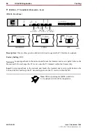
Page 69: ... 19 21 23 2 4 6 8 10 12 14 16 18 20 22 24 FXS Status Channel Data Loop 2 Lcl Off Net Data Loop 1 Lcl Off Net T1 Loop Net Off Lcl 1 Off 2 Off QRSS T1 Status T1 Loop Test Pattern Test Pattern T1 Test Self Check 11287 A ON Sync A Green LED indicates that the test pattern received by the Data Port 1 or 2 pattern detector matches the pattern generated by the system OFF No Sync Test Pattern 1 Off 2 ...
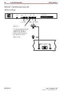
Page 70: ... 19 21 23 2 4 6 8 10 12 14 16 18 20 22 24 FXS Status Channel Data Loop 2 Lcl Off Net Data Loop 1 Lcl Off Net T1 Loop Net Off Lcl 1 Off 2 Off QRSS T1 Status T1 Loop Test Pattern Test Pattern T1 Test Self Check 11288 A ON Sync A Green LED indicates that the test pattern received by the Data Port 1 or 2 pattern detector matches the pattern generated by the system OFF No Sync Test Pattern 1 Off 2 ...
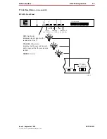
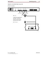
Page 71: ...CX 250 1 3 5 7 9 11 13 15 17 19 21 23 2 4 6 8 10 12 14 16 18 20 22 24 FXS Status Channel Data Loop 2 Lcl Off Net Data Loop 1 Lcl Off Net T1 Loop Net Off Lcl 1 Off 2 Off QRSS T1 Status T1 Loop Test Pattern Test Pattern T1 Test Self Check 11289 A BLINKING Call Processing ON Connected OFF Idle 1 3 5 7 9 11 13 15 17 19 21 23 2 4 6 8 10 12 14 16 18 20 22 24 FXS Status Channel ...

Page 72: ...G Technical Assistance Center at 1 800 366 3891 extension 3223 in U S A or Canada or 612 946 3223 outside U S A and Canada A telephone consultation can sometimes resolve a problem without the need to repair or replace the ADC Product If during a telephone consultation ADC determines the ADC Product requires repair ADC will authorize the return of the affected Product by the issue of a Return Mater...

Page 73: ... for any advance replacement credit If repairs necessitate a field visit by an ADC representative customer authorization purchase order must be obtained prior to dispatching a representative ADC will charge the current price of a field visit plus round trip transportation charges from Minneapolis to the customer s site REPLACEMENT SPARE PRODUCTS Replacement parts including but not limited to butto...

Page 74: ... ADC offers the following customer support services For calls originating in the U S A or Canada dial 1 800 366 3891 then request the extension listed For calls originating outside the U S A or Canada dial 612 946 3000 or 612 946 3223 BBG Technical Assistance Center Technical Information Extension 3223 System Network Configuration Product Specification Product Application Proposals Training Instal...

Page 75: ...indirect incidental special consequential or other similar damages This disclaimer of liability applies to all products publications and services during and after the warranty period This publication may be verified at any time by contacting ADC s Technical Assistance Center at 1 800 366 3891 extension 3223 in U S A or Canada or 612 946 3223 outside U S A and Canada or by writing to ADC Telecommun...

Reviews: