background image

12 / Chapter 3 Installation

USB

COM2

AMR SLOT

PCI SLOT2

PCI SLOT1

AGP1

JACK1

JACK2

JACK3

B :   K / B
T: Mouse

Printer

PANEL1

J3
J4

J6

FAN1

J2

JBAT1

JWOL1

FAN2

GAME1

BIOS

ISA SLOT1

VIA

VIA

COM1

CO

D

EC

CDIN1

BSEL1

BSEL0

JCK1

JCK2

JCK3

JCK4

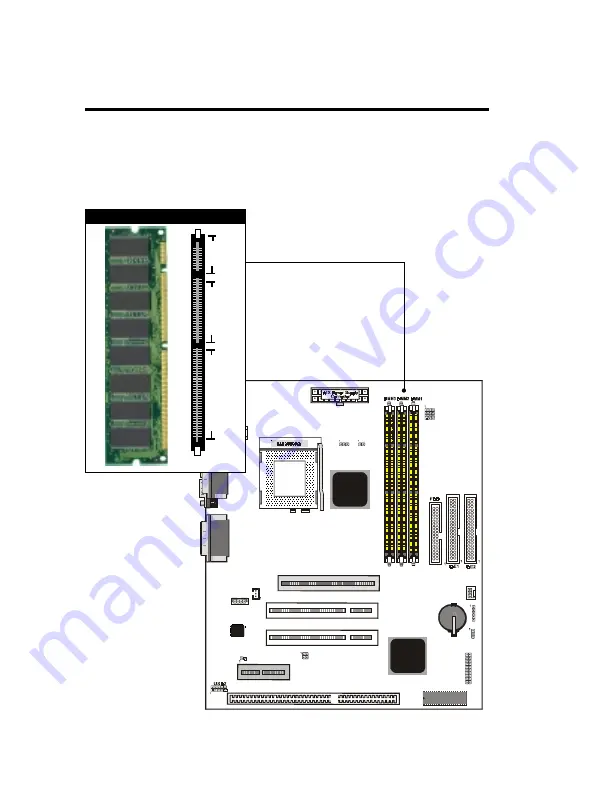
DIMM Memory Installation

Insert the module (s) as shown. Because the number pins are differ-
ent on either side of the breaks,the module will only fit in the orienta-
tion as shown. SDRAM DIMM modules have different pin contacts
on each side and therefore have a higher pin density.

168 Pin DIMM Socket

88 pins

60 pins

20 pins

Summary of Contents for 6VIA89

Page 1: ...roduction Manual information and checklist Chapter2 Features Information and Specifications con cerning this mainboard Chapter3 Installation Instructions on setting up the board The mainboard is a high performance mainboard based on the ad vanced Socket 370 microprocessor the VGA Audio PCI Bus and the VIA 694X chipset 1 Chapter 1 ...

Page 2: ...r package is complete If you discover any item damaged or missing please contact with your retailer immediately The 6VIA89 mainboard USB2 conector with bracket option 1 x IDE UDMA66 ribbon cable 1 x floppy ribbon cable 6VIA89 drivers and utilities This user s Manual ...

Page 3: ...VIA89 Mainboard VIA 694X chipset supports 66 100 133MHz FSB UltraDMA66 AGP4X mode SupportsIntel sprocessordesignedforsocket370andpackageinPPGA FCPGA IntegratedH Wmonitorcompensationengine support TouchButtonWakeup forsoftpoweron offandsus pendmodemultifunction ...

Page 4: ...he PCI IDE Controller supports PIO Mode 0 to Mode 4 Bus master IDE DMA Mode 2 and Ultra DMA66MB Support PS 2 mouse Connector System BIOS supports LS 120 ZIP driver firmware and Green feature function Plug and Play Flash ROM AC 97 DAC built into the audio CODEC reduces noise to im prove audio quality and performance for a SNR signal to noise ratio of 90dB These features greatly improve voice synthe...

Page 5: ... Jumper Refer to page JBAT1 CMOS Clear 10 BSEL0 1 CPU Type selection 15 JCK1 4 CPU bus frequency selection 16 J3 J4 On board AC 97 Selection 17 J2 AMR Type Selection 17 FAN1 FAN Connector 21 FAN2 FAN Connector 21 J6 IrDA Connector 22 WOL1 Lan Card Wake Up 26 ...

Page 6: ...t DOWN 20 COM1 COM 1 serial port 20 COM2 COM 2 serial port 20 USB Universal Serial BUS Ports 1 2 20 USB2 Universal Serial BUS Ports 3 4 20 PRINT Parallel port 20 FDC FLOPPY connector 20 IDE1 Primary IDE connector 21 IDE2 Secondary IDE connector 21 PANEL1 HDD LED 23 PANEL1 SMI Switch 23 PANEL1 Reset Switch 24 PANEL1 Speaker Connector 24 PANEL1 Power LED 24 PANEL1 ATX Power switch 24 PW1 ATX Power C...

Page 7: ... 6VIA89 Mainboard Layout USB COM2 AMR SLOT PCI SLOT2 PCI SLOT1 AGP1 JACK1 JACK2 JACK3 B K B T Mouse Printer PANEL1 J3 J4 J6 FAN1 J2 JBAT1 JWOL1 FAN2 GAME1 BIOS ISA SLOT1 VIA VIA COM1 C O D E C CDIN1 BSEL1 BSEL0 JCK1 JCK2 JCK3 JCK4 ...

Page 8: ...e Static Electricity Precaution Keep the mainboard and other system components in their anti static packaging until you are ready to install them Do all preparative work on a static free surface with the main board components facing up Unplug your computer when working on the inside Wear an Anti static wrist strap Hold the system components boards or cards by its edges only Be careful not to touch...

Page 9: ...n the left when holding the mainboard with the keyboard away from yourself P1 is written besides pin 1 on jumper with three pins The jumpers will also be shown graphically such as to connect pin 1 2 and to connect 2 3 Jumpers with two pins will be shown as for Short on and for Open off For manufacturing simplicity it may be sharing pins from other groups Use the diagrams in this manual instead of ...

Page 10: ...EL1 BSEL0 JCK1 JCK2 JCK3 JCK4 Real Time Clock RTC RAM JBAT1 The CMOS RAM is powered by the onboard button cell battery To clear the RTC data 1 Turn off your computer 2 Move this jumper to 2 3Pin Clear Data 3 Move the jumper back to Default 4 Turn on your computer 5 Hold down Delete during boot up and enter BIOS setup to re enter user Preferences JBAT1 CMOS Clear 1 2 default Normal 2 3 Clear CMOS P...

Page 11: ...IMM 1 16MB 32MB 64MB 128MB 256MB Bank 0 1 168 pin 3 3v SDRAM EDO RAM DIMM 2 16MB 32MB 64MB 128MB 256MB Bank 2 3 168 pin 3 3v SDRAM EDO RAM DIMM 2 16MB 32MB 64MB 128MB 256MB Bank 2 3 168 pin 3 3v SDRAM EDO RAM TotalSystemMemory Max768MB Note At the time this user s manual was written 256MB DIMM s are only available as double sided registered memory 128Mbit cells The motherboard operates at 133MHz t...

Page 12: ...VIA COM1 C O D E C CDIN1 BSEL1 BSEL0 JCK1 JCK2 JCK3 JCK4 DIMM Memory Installation Insert the module s as shown Because the number pins are differ ent on either side of the breaks the module will only fit in the orienta tion as shown SDRAM DIMM modules have different pin contacts on each side and therefore have a higher pin density 168 Pin DIMM Socket 88 pins 60 pins 20 pins ...

Page 13: ...nDRAMDIMMNotchKeyDefinitions The notch on the DIMM module will shift between left center or right to identify the type and also to prevent the wrong type to be inserted into the DIMM slot on the Mainboard You must ask your retailer for Specifications before purchasing Four clock signals are supported on this mainboard RFU Unbuffered Buffered 5 0V Reserved 3 3V DRAM Key Position Voltage Key Positio...

Page 14: ...a fan attached to it to prevent over heating If this is not the case then purchase a fan before you turn on your system To install a CPU first turn off your system and remove its cover Locate the ZIF socket and open it by first pulling the lever sideways away from the socket then upwards to a 90 degree right angle Insert the CPU with the correct orientation shown The notched corner should point to...

Page 15: ...s in limited to 33MHz socket370 Celeron processors limited to 66MHz and SDRAM limited to the DIMM type 66 100 133MHz 66MHz SDRAM is not supported on this motherboard Other settings are for experienced users only BSEL0 BSEL1 Auto detected by CPU 100Mhz Run 133Mhz test only 66Mhz Run 100Mhz test only 66MHz ONLY NOTE Most of the CPU frequency are locked by the manufacturer This motherboard is able to...

Page 16: ...equency Selection JCK1 JCK2 JCK3 JCK4 The JCK1 4 jumpers is used to set PCI and CPU external bus clock C L K P C I J C K 1 J C K 2 J C K 3 J C K 4 133 3 33 3 1 1 1 1 124 3 1 0 1 1 1 150 37 5 1 0 1 1 140 3 5 0 0 1 1 105 3 5 1 1 0 1 110 36 7 0 1 0 1 115 38 3 1 0 0 1 120 4 0 0 0 0 1 100 33 3 1 1 1 0 133 3 44 43 0 1 1 0 112 37 3 1 0 1 0 103 34 3 0 0 1 0 66 8 33 4 1 1 0 0 83 3 41 7 0 1 0 0 7 5 37 5 1 0...

Page 17: ...se Printer PANEL1 J3 J4 J6 FAN1 J2 JBAT1 JWOL1 FAN2 GAME1 BIOS ISA SLOT1 VIA VIA COM1 C O D E C CDIN1 BSEL1 BSEL0 JCK1 JCK2 JCK3 JCK4 Audio Modem Riser AMR Function Selection J2 J2 OFF Primary O N Secondary P1 P1 Onboard AC 97 Function Selection J3 J4 J3 J4 O N Disabled OFF Enabled P1 J3 J4 P1 J3 J4 ...

Page 18: ...The clearance on at least 3 of 4 sides of the processor and fan heatsink must be at least 0 2 inch All cables for Floppy drive Hard drive CD ROM and so on must be routed clear of the processor and its airspace Fan Exhaust The processor must be kept cool by using a processor with heatsink and fan attached The temperature of the air filled with the fan heatsink cannot exceed 45 O C 113 O F The ambie...

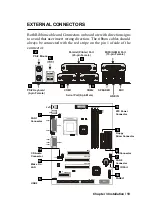
Page 19: ... with direction signs to avoid that user insert wrong direction The ribbon cables should always be connected with the red stripe on the pin 1 of side of the connector PS 2 Keyboard 6 pin Female Serial Port 9 pin Male COM1 COM2 SPEAKER MIC LINE IN PS 2 Mouse Parallel Printer Port 25 pin Female MIDI GAME Port 15 pin Female 1 2 5 3 4 3 Floppy Driver Connector 6 10 FAN 1 Connector 7 IR Port 9 CD Audio...

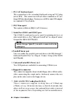
Page 20: ... must be connected to the serial port 4 Parallel Printer port You can enable the parallel port and choose the IRQ through Onboard Parallel Port in Chipset Feature Setup of the BIOS SOFTWARE 5 Universal Serial BUS Ports 1 2 Two USB ports are available for connecting USB devices 6 Floppydriveconnector This connector supports the provided floppy drive ribbon cable After connecting the single end to t...

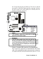
Page 21: ...e Rotation signal is to be used only by a specially de signed fan with rotation signal WARNING The CPU and or motherboard will overheat if there is no air flowing acrosstheCPUandonboardheatsinks Damagemay occurtothemotherboardand ortheCPUfaniftherepinsare incorrectlyused Thesearenotjumpers donotplacejumper caps over these pins 8 Primary Secondary IDE connectors Two 40 pin Blocks These connectors s...

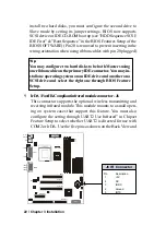
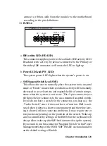
Page 22: ...sing ribbon cables with pin 20 plugged Tip You may configure two hard disks to be both Masters using oneribboncableontheprimaryIDEconnector Youmayin stall one operating system on an IDE drive and another on a SCSI drive and select the right one through BIOS Feature Setup 9 IrDA FastIR Compliantinfraredmoduleconnector J6 This connector supports the optional wireless transmitting and receiving infra...

Page 23: ...y and expand the life of certain compo nents when the system is not in use This 2 pin connector see the figure below connects to the case mounted suspend switch If you do not have a switch for the connector you may use the Turbo Switch since it does not have a function SMI is acti vated when it detects a short to open moment and therefore leav ing it shorted will not cause any problems It may requ...

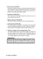
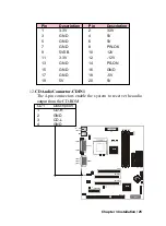
Page 24: ...speaker g ATX Power Switch PW_BN The system power is controlled by a momentary switch connected to this lead Pushing the button once will switch the system ON The system power LED lights when the system s power is on 11 ATX Power Supply Connector 20 pin block PW1 This connector connects to a ATX power supply The plug from the power supply will only insert in one orientation because of the differen...

Page 25: ...A VIA COM1 C O D E C CDIN1 BSEL1 BSEL0 JCK1 JCK2 JCK3 JCK4 Pin Description Pin Description 1 3 3V 2 3 3V 3 GND 4 5V 5 GND 6 5V 7 GND 8 PW OK 9 5VSB 10 12V 11 3 3V 12 12V 13 GND 14 PS ON 15 GND 16 GND 17 GND 18 5V 19 5V 20 5V 12 CDAudioConnector CDIN1 The 4 pin connectors enable the system to receive the audio output from the CD ROM CD1 Description 1 CD R 2 GND 3 CD L 4 GND ...

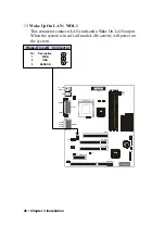
Page 26: ...AN1 J2 JBAT1 JWOL1 FAN2 GAME1 BIOS ISA SLOT1 VIA VIA COM1 C O D E C CDIN1 BSEL1 BSEL0 JCK1 JCK2 JCK3 JCK4 Pin Description 1 5VSB 2 GND 3 SENSOR Wake On LAN Connector P3 P1 13 Wake Up On LAN WOL1 This connector connects LAN cards and a Wake On LAN output When the system is in soft off mode LAN activity will power on the system ...

Page 27: ...et Technical Fault Report M B Model No Vender Serial No Date of Purchasing Hardware Configuration Used CPU RAM Video Card Hard Drive Other Card Diagnostic Software Used Fault Description Technical Support WWW www acorp com tw FAE fae acorp com tw ...

Reviews: