Manual PCI-A12-16A
18
Offset 4 Write
Option Control
This register is used to control various features on the card.
bit 7
bit 6
bit 5
bit 4
bit 3
Bit 2
bit 1
bit 0
XSCE
CCF
CF
EIFH
EIFE
CTR
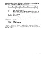
XSCE is External Start Conversion Enable. Setting this bit allows pin 4 on the connector to start conversions.
CCF and CF are Clear Channel FIFO and Clear FIFO (data) respectively. Any time a 1 is written to these bits,
the selected FIFO is reset, effectively clearing its contents.
EIFH set to 1 enables interrupts to occur when the data FIFO becomes Half Full. This is the interrupt most
often used in background-task-based data acquisition.
EIFE set to 1 enables interrupts on FIFO Error. That is, anytime the FIFO is read from when it is already
empty, or when data is lost because the FIFO is full when an A/D conversion finishes.
CTR set to 1 causes start conversions to occur each time counter 2 (used in Mode 2) counts down to zero.
The other bits in this register must be cleared to zero for compatibility with future options.
Offset 4 Read
Status, Clear Interrupt
This register is read to determine the status of various features on the card, primarily the state of the point-list
and data FIFOs, or to determine if a conversion has finished.
bit 7
bit 6
bit 5
bit 4
bit 3
bit 2
bit 1
bit 0
BUSY CFF CFH
CF0
FF FH F0 EXT
The BUSY bit indicates the conversion is in process. A zero means the A/D is busy, a one means a
conversion is not in progress. This bit is one of the most important when not using interrupt modes. By
reading this bit you can determine when the A/D conversion has finished and know when to take the data.
CFF, CFH, CF0, FF, FH, and F0 indicate when LOW that the respective status is true. (C)FF is FIFO Full,
(C)FH is FIFO Half Full, and (C)F0 means FIFO Empty.
The EXT bit works like a digital input bit. It shows the current state of the External Start A/D pin on the
connector (pin 4). A/D conversions can be started by pulling this pin high if XSCE is set to one in Offset 4.
Offset 8, 9, A, and B
8254 Counter / Timer
Refer to the 8254 section for information on programming this device.
Offset C & D
DAC 0
These registers are customarily written together in a single word write instruction. The value written is
immediately output on DAC 0.
Offset E & F
DAC 1
These registers are customarily written together in a single word write instruction. The value written is
immediately output on DAC 1.


