


ACCES I/O Products, Inc.
MADE IN THE USA
mPCIe-ISODIO-16 Uaser Manual
3
Rev B1
C
HAPTER
4:
C
ONFIGURATION
S
ETTINGS
There are no configuration settings on the mPCIe-ISODIO-16.
C
HAPTER
5:
PC
I
NTERFACE
This product interfaces with a PC using a PCI Express Mini Card
(mPCIe) connection; a small-form-factor, high-performance, rugged
peripheral interconnect technology first introduced for use in
laptops and other portable computers.
mPCIe’s small size and powerful performance, combined with
perfect software compatibility with PCI and PCIe peripheral designs,
have led to its recent adoption as a go-to standard for embedded
Data Acquisition and Control, and many other applications.
Although mPCIe is a broadly-adopted industry standard, the actual
connection to the computer shares a specification with mSATA:
both mSATA and mPCIe use the same edge-connector. In fact, well-
designed PCs can automatically detect and configure their onboard
connectors to work with either mPCIe or mSATA devices – and,
according to the standards for mPCIe and mSATA they are
supposed
to do so! However, some PC manufacturers ship computers that
only
support mSATA devices. Please confirm in your PC
documentation that your edge-connector is
actually
PCI Express
Mini Card compliant before installing this, or any, mPCIe card.
Damage might occur if you install an mPCIe device into a computer
that only supports mSATA.
mPCIe defines mounting holes for securing the otherwise loose end
of the card, so it is impossible for these cards to wiggle or flap
themselves loose (which was a recurring problem with the older PCI
Mini devices). Eliminating this concern for PCI Express Mini Cards is
a major reason this standard has seen rapid adoption by the Data
Acquisition and Control industry.
The mPCIe standard, like its PCI Mini Card predecessor, was
designed assuming use primarily in Laptop or Notebook and similar
devices, where physical dimension is often the paramount design
constraint. In Data Acquisition and Control applications low-weight
combined with vibration tolerance tend to be of more concern.
C
HAPTER
6:
I/O
I
NTERFACE
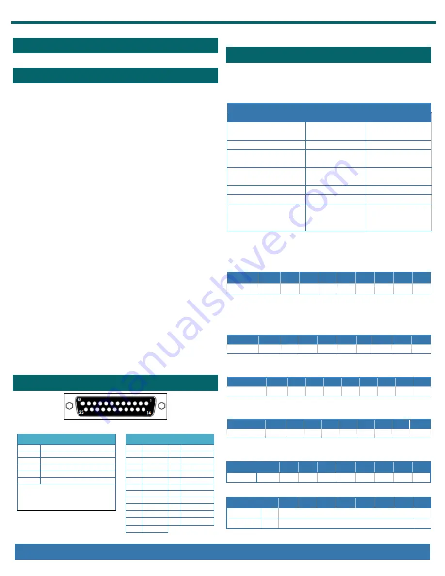
DB25F Pinouts on CAB-mPCIe-ISODIO cable assembly
Signal Definitions
DB-25 Female Pinout
Signal
Meanings
1
IN 0
14
OUT 0
IN
Isolated Input
2
IN 1
15
OUT 1
OUT
Isolated Output
3
IN 2
16
OUT 2
ISOGND
Isolated Ground
4
IN 3
17
OUT 3
VCCIO
Fused Is3.3VDC @ 0.05A*
5
IN 4
18
OUT 4
N/C
No Connection
6
IN 5
19
OUT 5
*Keep cumulative power draw from I/O
sourcing and VCCIO <50mA
7
IN 6
20
OUT 6
8
IN 7
21
OUT 7
9
N/C
22
N/C
10
N/C
23
N/C
11
ISOGND
24
N/C
12
ISOGND
25
VCCIO
13
ISOGND
Custom hardware interfaces can be produced to fit your specific
application requirement.
C
HAPTER
7:
S
OFTWARE
I
NTERFACE
The simplest way to program for the device is using legacy-
compatibility mode: the device boots into this mode. In this mode,
the unit provides I/O-mapped registers: 2 DIO registers, enable
register and a 32-bit register for the Watchdog Timer.
I/O Registers at BAR [2]
Register offset (hex)
Write Operation
Read Operation
Isolated Outputs [ + 0 ]
0-7 output
Output 0-7 read-
back
Isolated Inputs [ + 1 ]
unused
Input 0-7 input
Buffer Enable [ + A ]
Control DIO Buffer
Enable
DIO Buffer Enable
Read-back
Cos Mask [ + B ]
Change-of-State
Enable
Change-of-State
Enable Read-back
IRQ Clear [ + F ]
Clear IRQ
unused
IRQ Clear/Status [ + 29 ]
Clear IRQ
IRQ Status
Watchdog Timer
[+30..+33 ]
32-bit Watchdog
Timeout Duration
Divisor
Read-back of
Watchdog Timeout
Duration Divisor
In the following bit-level register descriptions the column labeled
“Dir” indicates read or write operation, with the following notation:
R: Read function, and W: Write function. RW indicates both.
r: read, and w: write, but less-commonly useful than R or W
+ 0
Dir
D7
D6
D5
D4
D3
D2
D1
D0
Out #
rW
7
6
5
4
3
2
1
0
Writing one byte to +0 will control all 8 isolated outputs. Setting a
bit to 1 sets the corresponding isolated output, while clearing a bit
to 0 turns it off. Reading a byte will provide the currently
commanded output state (read-back).
+ 1
Dir
D7
D6
D5
D4
D3
D2
D1
D0
In #
R
7
6
5
4
3
2
1
0
Reading from +1 returns 8 bits. Each bit indicates the level that was
detected at the corresponding isolated input.
+ A
Dir
D7
D6
D5
D4
D3
D2
D1
D0
ENABLE
RW
EN
Setting a bit to 1 at D0 at this register disables the DIO buffer, while
clearing the bit to 0 enables it.
+ B
Dir
D7
D6
D5
D4
D3
D2
D1
D0
ENABLE
RW
CoS
Setting a bit to 1 at D0 at this register masks the Change-of-State
for the inputs, while clearing the bit to 0 enables it.
+ F
Dir
D7
D6
D5
D4
D3
D2
D1
D0
Clear
W
0
Writing any value to +F clears all pending IRQ source latches.
+ 29
Dir
D7
D6
D5
D4
D3
D2
D1
D0
IRQ Clr
W
Write 0xFF to clear pending IRQs
IRQ Stat
R
INT


