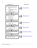


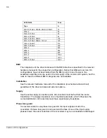

25
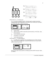
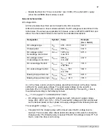
The peak current during charging is calculated by the equation in
Checking the
charging capacity
.
Charging time is longer if a higher resistance value is used.
It must be checked that AC supply side components can withstand the peak current.
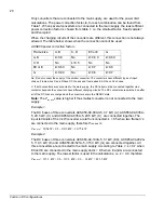
Charging resistor energy withstand is calculated by equation E = 1.3CU
2
where C is
total capacitance of DC-link capacitors and U is supply line-to-line rms voltage for
example 400 V or 500 V. The factor 1.3 covers the upper tolerance limit of
capacitance.
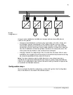
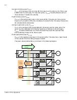
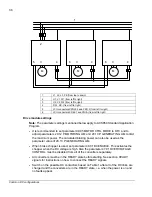
If drive units with different charging circuits are used, the DC-links must be connected
together via contactors.
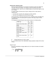
Frame sizes A…D
If only frames A…D are used, there is no need for an external charging circuit with the
external DC supply, because the drive modules have internal charging circuits in series
with DC-link capacitors.
Frame sizes E0, E and G
In frame sizes E0, E and G, the charging circuit is in parallel with the input bridge.
Separate charging circuit is needed.
The AC fan of ACS850 frame G must be powered separately. See chapter
Powering
the AC fan in frame G
.
Supply units other than ACS850
When some other type of supply unit than ACS850 is used, its DC voltage compatibility
with the drive units must be checked in addition to the earlier described items (see
section
DC voltage limits
).
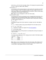
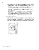
Mains choke selection
In common DC connections, the drive module(s) connected to the AC supply must be
equipped with mains choke(s). The mains chokes are needed:
•
to get the maximum DC power ratings from the drive module(s)
•
to reduce the AC input current (rms, peak) level
•
to meet the requirements for harmonic distortion
•
to balance the supply current in a multiple AC input.
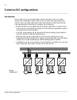
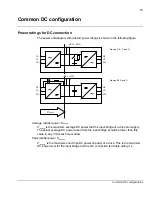
Common DC configurations
Summary of Contents for ACS850 series
Page 1: ...ACS850 Common DC configuration application guide...
Page 2: ......
Page 4: ......
Page 6: ...6 Safety instructions...
Page 9: ...9 Table of contents...
Page 11: ...11 Introduction to the manual...


