background image

UM008 FMC204 User Manual 


r1.14


UM008


www.4dsp.com


- 26 - 

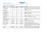
Field 

Description 

DIRx 

Direction of Front IO transceiver (x = 0 to 3) 


‘0’ 

Signal x is input (FMC204 is receiver) 


‘1’ 

Signal x is output (FMC204 is transmitter) 

FANx 

Power control for FAN header  (x = 0 to 3) 


‘0‘ 

Apply power to FAN header x 


‘1‘ 

Cut power to FAN header x 

Table 13: Register CPLD_REG1 description 


Bit nr. 

Bit 7 

Bit 6 

Bit 5 

Bit 4 

Bit 3 

Bit 2 

Bit 1 

Bit 0 

Name 

Reserved 

IRQ 

VM 

STATUS 

LD 

REFMON 

Table 14: Register CPLD_REG2 definition (read) 


Field 

Description 

REFMON 

Reflect the status of the REFMON output of the AD9517 

LD 

Reflect the status of the LD output of the AD9517 

STATUS 

Reflect the status of the STATUS output of the AD9517 

VM 

Reflect the status of the INT# output of the ADT7411 (inverted) 


‘0‘ 

INT# is not asserted 


‘1‘ 

INT#  is  asserted,  access  to  the  ADT7411  trough  the  I

2

C  bus  is  required  to 

determine the source of the interrupt 

IRQ 

Logic function: 

NOT

 (REFMON 

AND

 LD 

AND

 STATUS 

AND

 INT#) 


‘0‘ 

All status signals indicate OK 


‘1‘ 

One or more status signals indicate ERROR 

Table 15: Register CPLD_REG2 description (read) 


Bit nr. 

Bit 7 

Bit 6 

Bit 5 

Bit 4 

Bit 3 

Bit 2 

Bit 1 

Bit 0 

Name 

Reserved 

LED_SEL 

Table 16: Register CPLD_REG2 definition (write) 


Summary of Contents for FMC204

Page 1: ...UM008 www 4dsp com 1 FMC204 User Manual 4DSP LLC USA Email support 4dsp com This document is the property of 4DSP LLC and may not be copied nor communicated to a third party without the written permis...

Page 2: ...ICTOR connector references 1 5 2011 03 09 Added coax connector type specification 1 6 2011 04 14 Added FMC connector type specification Updated trigger input specification 1 7 2011 08 01 Update extern...

Page 3: ...rical specifications 8 4 2 1 EEPROM 8 4 2 2 JTAG 8 4 2 3 FMC HPC 8 4 3 Main characteristics 10 4 4 Analog output channels 10 4 5 External clock input 10 4 6 External trigger sync input 11 4 7 Clock Tr...

Page 4: ...TAG Join Test Action Group LED Light Emitting Diode LVTTL Low Voltage Transistor Logic level LSB Least Significant Bit s LVDS Low Voltage Differential Signaling MGT Multi Gigabit Transceiver MSB Most...

Page 5: ...a SPI communication bus The FMC204 card is equipped with power supply and temperature monitoring with several power down modes to switch off unused functions to reduce system level power and heat The...

Page 6: ...3V for FMC204 revision 2 but typically VADJ will be 1 8V or 2 5V for LVDS operation Do not flex the card Prevent electrostatic discharges by observing ESD precautions when handling the card 3 2 LVDS r...

Page 7: ...MI I O The 19 pins HDMI connector on the front panel IO holds four multi gigabit transceivers two Tx pairs two Rx pairs and 4x LVTTL I O 5V tolerant Contact 4DSP for other configurations Pin Number Si...

Page 8: ...ther status and control signals like serial communication busses operate at LVCMOS level VOH VADJ 4 2 1 EEPROM The FMC204 card carries a 2Kbit EEPROM which is accessible from the carrier card through...

Page 9: ...DS Clock 1 1 LVDS Trigger 1 1 LVDS Sync 1 1 DAC 1 18 LVDS Clock 1 LVDS Sync 1 LVDS Data 16 DAC 2 17 LVDS Clock 1 LVDS Sync 0 LVDS Data 16 2 5V or VADJ Level I O routed to CPLD see board revision 0 4 T...

Page 10: ...511 000 Frequency range Up to 500 MHz DAC input Input data width 1x 16 pairs DDR 1Gbps Data Format Two s Complement Offset binary FMC connector type HPC ASP 134488 01 Sampling Frequency Range 100 1000...

Page 11: ...topology Synchronization of multiple D A devices in parallel is done through the SYNC input The SYNC signal is driven by the FPGA and can be derived from the trigger input Since the SYNC input has an...

Page 12: ...input of the AD9517 or the 2nd RF switch CLKSRC_SEL1 connect either the onboard VCXO or the external clock to the clock input of the AD9510 This signal also controls the VCXO power supply2 CLKSRC_SEL2...

Page 13: ...com 13 5Rx 5Tx 5Rx 5Tx 5Rx 5Tx 5Rx 5Tx 5Rx 5Tx 5Rx 5Tx 5Rx 5Tx 5Rx 5Tx 5Rx 5Tx 5Rx 5Tx Figure 5 MGT interconnect topologies FMC 20 32 10 00 7 12 13 71 FPGA MICTOR 2 Rx Tx 5 9 MICTOR 1 Rx Tx 0 4 TOP VI...

Page 14: ...RX4_N 30 29 RX5_N GND TX5_N 30 31 GND GND GND 32 31 GND GND GND 32 33 IO0 GND 34 33 IO2 GND 34 35 IO1 GND 36 35 IO3 GND 36 37 GND GND GND 38 37 GND GND GND 38 Table 5 MGT connector pin out3 A low phas...

Page 15: ...here is additional noise filtering at several stages in the power supply The regulators have sufficient copper area to dissipate the heat in combination with proper airflow see section 6 3 Cooling Pow...

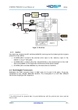
Page 16: ...stribute SPI access from the carrier hardware along the local devices 2x DAC5682Z D A converters 1x AD9517 Clock Tree Select clock source based on a SPI command from the carrier hardware CLKSRC_SEL Se...

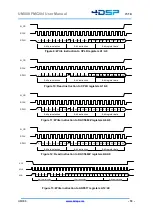
Page 17: ...ted N_SYNC on the AD9517 on the revision 1 boards is not connected On revision 2 boards N_SYNC is connected to the CPLD for future use N_RESET on the both DAC5682Z devices is shared 5 2 SPI Programmin...

Page 18: ...s A1 A0 8 bit pre selection P6 P5 P4 P3 P2 P1 P0 R W N1 N0 A4 A3 A2 A1 A0 8 bit instruction 8 bit register data D7 D6 D5 D4 D3 D3 D1 D0 N_CS SCLK SDIO P7 Figure 11 Write instruction to DAC5682Z regist...

Page 19: ...ferent power rails as well as the ambient temperature around the monitoring device It is recommended that the carrier card and or host software uses the power down features if the temperature is too h...

Page 20: ...anding environments the ambient temperature inside a chassis could be close to the operating temperature defined in this document It is very likely that in these conditions the junction temperature of...

Page 21: ...UM008 www 4dsp com 21 9 Warranty Hardware Software Firmware Basic Warranty included 1 Year from Date of Shipment 90 Days from Date of Shipment Extended Warranty optional 2 Years from Date of Shipment...

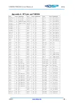
Page 22: ...P E33 N C LA06_N C11 N C HA10_N K14 N C HB20_N F38 FRONT_IO_FMC 1 LA06_P C10 N C HA10_P K13 N C HB20_P F37 FRONT_IO_FMC 0 LA07_N H14 N C HA11_N J13 N C HB21_N E37 FRONT_IO_FMC 3 LA07_P H13 N C HA11_P...

Page 23: ...H29 DAC0_DATA_P 6 HB04_N F26 DAC1_DATA_P 10 DP7_C2M_N B33 DP_C2M_N 7 LA24_P H28 DAC0_DATA_N 6 HB04_P F25 DAC1_DATA_N 10 DP7_C2M_P B32 DP_C2M_P 7 LA25_N G28 DAC0_DATA_P 7 HB05_N E25 DAC1_DATA_P 13 DP7...

Page 24: ..._P N DDR DAC_SYNC_N DAC_SYNC_P D A 0 D A 1 Input LVDS Signal used as transmit enable for both DACs TRIGGER_TO_FPGA_N TRIGGER_TO_FPGA_P TRIGGER Output LVDS Representation of the signal connected to the...

Page 25: ...SYNCSRC Selection of synchronisation source 00 External Trigger 01 Carrier trough SYNC_FROM_FPGA_P N 10 Clock Tree 11 No Sync CLKR Clock tree SPI reset 0 Normal operation 1 Reset resetting the clock...

Page 26: ...Description REFMON Reflect the status of the REFMON output of the AD9517 LD Reflect the status of the LD output of the AD9517 STATUS Reflect the status of the STATUS output of the AD9517 VM Reflect th...

Page 27: ...4 UM008 www 4dsp com 27 Field Description LED_SEL Writing to this register determines which status signal is indicated by the LED XXXX1 REFMON XXX10 LD XX100 STATUS X1000 VM 10000 IRQ Table 17 Registe...

Reviews: