background image

UM027 FC6301 User Manual 


r1.3


UM027


www.4dsp.com


- 1 - 


FC6301 

User Manual 


4DSP LLC, USA 


Email: 

[email protected]


This document is the property of 4DSP LLC and may not be copied nor communicated to a 

third party without the written permission of 4DSP LLC 


© 4DSP LLC 2013 


Summary of Contents for FC6301

Page 1: ... UM027 www 4dsp com 1 FC6301 User Manual 4DSP LLC USA Email support 4dsp com This document is the property of 4DSP LLC and may not be copied nor communicated to a third party without the written permission of 4DSP LLC 4DSP LLC 2013 ...

Page 2: ...ease 1 0 2013 04 08 Added the FMC pinout tables 1 1 2013 05 01 Updated Table 5 FMC GTX GTH connections to use the MGTx_abc notation Also fixed wrong reference to MGT bank 115 and changed it to MGT bank 113 1 2 2014 04 15 Added Table 2 P2 connections and updated section 4 1 with a description of the P2 connector limitation 1 3 ...

Page 3: ... 4 4 FPGA Mezzanine Card FMC 12 4 4 1 Bank A LA HA connections 12 4 4 2 Bank B HB connections 15 4 4 3 Gigabit transceiver connections 16 4 4 4 Miscellaneous FMC connections 17 4 5 SPI flash 18 4 6 Virtex 6 FPGA device 18 4 7 BLAST sites 19 4 8 Clock tree 19 4 8 1 FMC GTX Reference Clock 20 4 8 2 FMC Clock connections 20 4 9 FPGA device configuration 21 4 9 1 Flash storage 21 4 9 2 CPLD device 21 ...

Page 4: ...UM027 FC6301 User Manual r1 3 UM027 www 4dsp com 4 Appendix A Errata 27 ...

Page 5: ...er Interface HPC High pin count IP Intellectual Property JTAG Join Test Action Group LED Light Emitting Diode LSB Least Significant Bit s LVDS Low Voltage Differential Signaling LVTTL Low Voltage Transistor Logic level MGT Multi Gigabit Transceiver MSB Most Significant Bit s PCB Printed Circuit Board PCI Peripheral Component Interconnect PCIe PCI Express PLL Phase Locked Loop pps Pulse Per Second ...

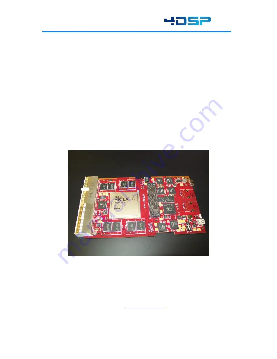
Page 6: ...ng DSP applications The FC6301 product is in the 3U cPCI form factor offering various direct on board interface options that are closely coupled to large fast on board memory resources of the Xilinx Virtex 6 FPGA The FC6301 is an excellent choice for high performance applications that require the use of accelerated frequency domain algorithms such as with FFTs 4DSP has many off the shelf Intellect...

Page 7: ...al Gigabit 3 Ethernet 2x optional Mini USB UART 128Mbit SPI flash2 72 single ended user defined IO4 160 single ended 80 LVDS pairs Figure 1 FMC122 block diagram 1 4th BLAST site only fully supported on SX475T and LX550T devices on other devices only the DDR2 BLAST A is supported 2 Refer to the Appendix for Errata 3 FMC and Ethernet are mutually exclusive Either Ethernet or FMC can be used 4 Defaul...

Page 8: ... firmware please refer the 4FM Get Started Guide 4 Hardware Specification 4 1 Phycisal specifications The FC6301 card complies with the compact PCI standard known as PICMG 2 0 R3 0 The card is a 3U 100 mm by 160 mm module which incorporates a 32 bits PCI bus on the P1 connector The P2 connector is fully routed to the Virtex6 FPGA through zero ohm resistors However the LX240T version of the Virtex6...

Page 9: ... D7 FP_RTM_23 1 8V Not available on LX240T AL24 D9 FP_RTM_24 1 8V Not available on LX240T BA25 D11 FP_RTM_25 1 8V Not available on LX240T AN24 E1 FP_RTM_26 1 8V Not available on LX240T AN25 E2 FP_RTM_27 1 8V Not available on LX240T AV26 E3 FP_RTM_28 1 8V Not available on LX240T AU26 E4 FP_RTM_29 1 8V Not available on LX240T AJ22 A7 FP_RTM_3 1 8V Not available on LX240T AR24 E5 FP_RTM_30 1 8V Not a...

Page 10: ...FP_RTM_58 1 8V Not available on LX240T C26 C20 FP_RTM_59 1 8V Not available on LX240T AM22 A10 FP_RTM_6 1 8V Not available on LX240T D26 C21 FP_RTM_60 1 8V Not available on LX240T M22 D13 FP_RTM_61 1 8V Not available on LX240T B26 D15 FP_RTM_62 1 8V Not available on LX240T C25 D17 FP_RTM_63 1 8V Not available on LX240T N23 D19 FP_RTM_64 1 8V Not available on LX240T M24 D21 FP_RTM_65 1 8V Not avail...

Page 11: ...nt panel IO options Not all can be used simultaneously In case an FMC is used no Ethernet connection is possible 4 3 1 Gigabit Ethernet Two Ethernet ports RJ45 connectors are available on the FC6301 in the front panel I O area The FPGA is connected to a 2 port Ethernet PHY 88E1121 that connects to two RJ45 connectors The Gigabit Ethernet ports are capable to adapt to lower Ethernet speeds 10 100 i...

Page 12: ...ections Differential routing is applied with matched delay within pairs on bank A LA HA FPGA Pin Net Name FMC HPC Pin Number Pin Name AF30 LA_N00_CC G7 LA00_N_CC AE30 LA_P00_CC G6 LA00_P_CC AK37 LA_N01_CC D9 LA01_N_CC AJ37 LA_P01_CC D8 LA01_P_CC AK30 LA_N02 H8 LA02_N AJ31 LA_P02 H7 LA02_P AJ32 LA_N03 G10 LA03_N AK33 LA_P03 G9 LA03_P AG29 LA_N04 H11 LA04_N AH29 LA_P04 H10 LA04_P AG39 LA_N05 D12 LA0...

Page 13: ...LA_N21 H26 LA21_N V31 LA_P21 H25 LA21_P W33 LA_N22 G25 LA22_N V33 LA_P22 G24 LA22_P W41 LA_N23 D24 LA23_N V41 LA_P23 D23 LA23_P W40 LA_N24 H29 LA24_N V40 LA_P24 H28 LA24_P W38 LA_N25 G28 LA25_N V38 LA_P25 G27 LA25_P V36 LA_N26 D27 LA26_N W36 LA_P26 D26 LA26_P V35 LA_N27 C27 LA27_N W35 LA_P27 C26 LA27_P U41 LA_N28 H32 LA28_N U42 LA_P28 H31 LA28_P V39 LA_N29 G31 LA29_N U39 LA_P29 G30 LA29_P U38 LA_N...

Page 14: ...11 HA06_N AH39 HA_P06 K10 HA06_P AH41 HA_N07 J10 HA07_N AG42 HA_P07 J9 HA07_P AG41 HA_N08 F11 HA08_N AF40 HA_P08 F10 HA08_P AF36 HA_N09 E10 HA09_N AF35 HA_P09 E9 HA09_P AF34 HA_N10 K14 HA10_N AG34 HA_P10 K13 HA10_P AD41 HA_N11 J13 HA11_N AC41 HA_P11 J12 HA11_P AE39 HA_N12 F14 HA12_N AE40 HA_P12 F13 HA12_P AE35 HA_N13 E13 HA13_N AE34 HA_P13 E12 HA13_P AD33 HA_N14 J16 HA14_N AE33 HA_P14 J15 HA14_P A...

Page 15: ... bank B HB FPGA Pin Net Name FMC HPC Pin Number Pin Name P38 HB_N00_CC K26 HB00_N_CC R39 HB_P00_CC K25 HB00_P_CC M37 HB_N01 J25 HB01_N M36 HB_P01 J24 HB01_P L40 HB_N02 F23 HB02_N L39 HB_P02 F22 HB02_P M39 HB_N03 E22 HB03_N M38 HB_P03 E21 HB03_P L42 HB_N04 F26 HB04_N L41 HB_P04 F25 HB04_P N39 HB_N05 E25 HB05_N N38 HB_P05 E24 HB05_P P35 HB_N06_CC K29 HB06_N_CC P36 HB_P06_CC K28 HB06_P_CC P37 HB_N07 ...

Page 16: ... E36 HB21_P Table 5 FMC HB connections 4 4 3 Gigabit transceiver connections The FC6301 connects the ten DP signals on the FMC connector to gigabit transceivers GTX blocks on the FPGA The reference clock connections are described in section 4 8 1 FPGA Pin Net Name GTX Block FMC HPC Pin Number Pin Name AP4 DP_C2M_N0 MGT0_112 C3 DP0_C2M_N AP3 DP_C2M_P0 C2 DP0_C2M_P AN6 DP_M2C_N0 C7 DP0_M2C_N AN5 DP_...

Page 17: ..._C2M_N7 MGT2_113 B33 DP7_C2M_N AH3 DP_C2M_P7 B32 DP7_C2M_P AE6 DP_M2C_N7 B13 DP7_M2C_N AE5 DP_M2C_P7 B12 DP7_M2C_P AK4 DP_C2M_N8 MGT0_113 B37 DP8_C2M_N AK3 DP_C2M_P8 B36 DP8_C2M_P AG6 DP_M2C_N8 B17 DP8_M2C_N AG5 DP_M2C_P8 B18 DP8_M2C_P AM4 DP_C2M_N9 MGT2_112 B37 DP9_C2M_N AM3 DP_C2M_P9 B36 DP9_C2M_P AL6 DP_M2C_N9 B17 DP9_M2C_N AL5 DP_M2C_P9 B18 DP9_M2C_P Table 6 FMC GTX GTH connections 4 4 4 Misce...

Page 18: ...e Virtex 6 device This flash allows the storage of vital data like processor boot code and settings into a non volatile memory The flash is operated using a standard SPI interface that can run up to 104 MHz allowing for a page programming speed up to 208 KB s Reading data from the flash can be done at speeds up to 13 MB s The SPI programming pins will be connected to a bank that supports 1V8 where...

Page 19: ...e 9 BLAST Configuration Options BLAST SITE 1 2 3 4 DDR3 YES YES YES YES DDR2 YES YES YES YES QDR YES YES YES YES ADV212 JPEG2000 YES YES YES YES 32GB NAND FLASH YES YES YES YES Table 10 BLAST Memory Processing Options 4 8 Clock tree The FC6301 clock architecture offers an efficient distribution of low jitter clocks A 100 MHz clock from a low jitter oscillator is distributed to the FPGA and the PCI...

Page 20: ...ference clocks FPGA Pin Net name GTX REFCLK GTX GTHs reached AK7 GBTCLK0_M2C_n GTXREFCLK0_112 112 113 AK8 GBTCLK0_M2C_p AD7 GBTCLK1_M2C_n GTXREFCLK1_113 112 113 114 AD8 GBTCLK1_M2C_p Table 11 FMC GTX reference clock connections 4 8 2 FMC Clock connections The FMC clocks are connected to LVDS capable I O on the FPGA CLK0 and CLK1 are connected to global clock inputs CLK2 and CLK3 are connected to r...

Page 21: ...he host motherboard via the PCI bus to the Virtex 6 device and then to the CPLD that writes the required bit stream to the storage device A 50MHz clock connects to the CPLD and is used to generate the configuration clock sent to the FPGA device At power up if the CPLD detects that an FPGA configuration bitstream is stored in the flash it will start programming the FPGA device in SelectMap mode The...

Page 22: ...itstream was detected in the user configuration space Please write a valid Virtex 6 device A bitstream to the flash ON Flash is busy writing or erasing OFF Flash device is not busy LED 3 ON CRC error Presumably a wrong or corrupted FPGA bitstream has been written to the flash Once on this LED remains on OFF No CRC error detected Table 14 LED board status 4 9 5 JTAG A JTAG connector footprint is av...

Page 23: ...10DN SI7110DN 0 004 0 004 3v3 to 2v5 1v2 EN5365QI FMC 3 A FMC_Vadj BLAST voltage 4 1v5 1v8 6 A 3v3 2A BLAST voltage 4 1v5 1v8 4 A 3v3 5v to 1v8 EP5396Q1 MGT 1 8A pericom 0 5A BLAST 4A 1v2 3v3 to 1v0 EP5396Q1 V6 8A 1v0_FP 1v8 to 1v2 TPS74401 1v8 to 1v5 TPS74401 1v8_FP 1v0 1v2 to 1v0 TPS74401 TPS2420 12V 3v3 to 1v0 EP5396Q1 V6 8A Figure 8 FC6301 power distribution Device Interface Voltage Maximum su...

Page 24: ...hot swap is not supported A hot swap controller is required to monitor all power levels pre charge the cPCI signals and to switch the backend power on and off The LTC1643A hot swap controller from linear technologies is used For more information on hot swap refer to the hot swap specifications 4 12 Power and temperature monitor Two ADT7411 devices are used to monitor the power on the different vol...

Page 25: ...T7411 Die Temperature On chip AIN0 VDD 3 3V External AIN1 BLAST0_vcore AIN1 External AIN2 BLAST2_vcore AIN2 External AIN3 5V AIN3 1249 249 External AIN4 0V9 AIN4 External AIN5 VADJ AIN5 External AIN6 1V8 AIN6 External AIN7 12V current Tbd External AIN8 2V5 AIN8 Table 17 monitoring device 2 connections ...

Page 26: ...ded to blow air across the FMC and ensure that the temperature of the devices is within the allowed range 4DSP s warranty does not cover boards on which the maximum allowed temperature has been exceeded 6 Safety This module presents no hazard to the user 7 EMC This module is designed to operate from within an enclosed host system which is build to provide EMC shielding Operation within the EU EMC ...

Page 27: ...UM027 FC6301 User Manual r1 3 UM027 www 4dsp com 27 Appendix A Errata PCB revision 2 1 SPI FLASH not supported ...

Reviews: