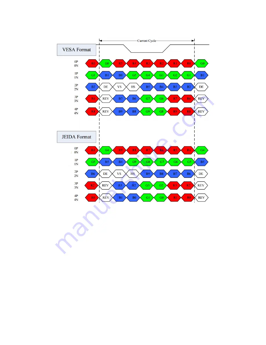
LVDS BIT MAPPING
The mapping of bits onto the LVDS signal lanes is shown here for both VESA and JEIDA
modes. For the color channels, bit 9 is the MSB and bit 0 is the LSB. REV signals are reserved and
are ignored by the system. DE, VSY, and HSY are the standard data-enable, vertical-sync, and
horizontal-sync signals.
LVDS PIXEL MAPPING
There are four input connectors, labeled INPUT1, INPUT2, INPUT3, and INPUT4, with each
input connector containing two LVDS channels. These eight channels can be called E1, O1, E2, O2,
E3, O3, E4, and O4. Within each group, four channels are interleaved to form the incoming pixel
stream. Beginning with pixel 0 in the upper left, E1 carries pixels 0, 4, 8, 12…, E2 carries 1, 5, 9,
13…, O1 carries 2, 6, 10, 14…, and O2 carries 3, 7, 11, 15... TODO: verify if correct ordering
“UHD TCON for Innolux Panels” User Guide ZisWorks.com Page 9/11


