background image

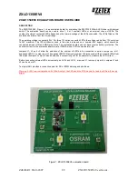
ZXLD1350EV4


Zdb346R1. 05-01-2007 

2/8 

ZXLD1350EV4 User Guide 


ZXLD1350 DEVICE DESCRIPTION 

The ZXLD1350 is a continuous mode inductive driver in a TSOT23-5 package, for driving one or more series 
connected LEDs efficiently from a voltage source higher than the LED voltage.  The device includes the output 
switch and a current sense circuit, which requires an external sense resistor to set the nominal current up to 
350mA.  

ZXLD1350 DEVICE FEATURES 


Drives one or more series-connected 1W white 
LEDs up to 350mA. 

 Internal 

30V 

switch. 


Wide input voltage: 7V to 30V. 


Inherent open circuit LED protection. 


Brightness control using DC or PWM. 

 Internal 

PWM 

filter. 

DEVICE APPLICATIONS


 LED 

flashlights. 


High Power LED driving. 


Low-voltage halogen replacement LEDs. 

 Automotive 

lighting. 

 Illuminated 

signs. 


ZXLD1350 Device Packages, Pin and Definitions 


TSOT23-5 pack


ZXLD1350 Device Pin Definition 
Name Pin 

No 

Description 

LX 1 

Drain 

of 

NDMOS 

switch. 

GND 2 

Ground 

(0V). 

ADJ 

Internal voltage ref. pin (1.25V) : 


Leave floating for normal operation. 


Connect to GND to turn off output current. 


Drive with DC voltage (0.3V to 1.25V) or with PWM signal to adjust 
output current or.... 


Connect a capacitor from this pin to ground to set soft-start time. 

ISENSE 

Connect a sense resistor, Rs,


from the ADJ pin to VIN to sense the nominal 

output current. Nominal I

out

 = 0.1/ Rs 

VIN 

Input voltage: 7V to 30V. Decouple to ground with a 1uF or higher ceramic 
capacitor. 


ORDERING INFORMATION 

EVALBOARD ORDER NUMBER 

ZXLD1350EV4 


Please note: Evaluation boards are subject to 
availability and qualified leads. 


DEVICE ORDER NUMBER 

ZXLD1350E5TA 


Содержание ZXLD1350EV

Страница 1: ... should be connected across VIN and GND pins Note The evaluation board does not have reverse battery protection The nominal current for the evaluation board is set at 300mA with a 0 33Ω sense resistor Rs Jumpers J1 J2 and J3 allow the selection of the number of LEDs to be connected in series Jumper on at J1 bypasses LED D1 Jumper on at J3 bypasses LED D3 Removing jumper J2 disconnects all the on b...

Страница 2: ...Power LED driving Low voltage halogen replacement LEDs Automotive lighting Illuminated signs ZXLD1350 Device Packages Pin and Definitions TSOT23 5 pack ZXLD1350 Device Pin Definition Name Pin No Description LX 1 Drain of NDMOS switch GND 2 Ground 0V ADJ 3 Internal voltage ref pin 1 25V Leave floating for normal operation Connect to GND to turn off output current Drive with DC voltage 0 3V to 1 25V...

Страница 3: ... be nominally 0 5ms without capacitor C3 Adding C3 will increase the soft start time by approximately 0 5ms nF For other reference designs or further applications information please refer to the ZXLD1350 datasheet Schematic Diagram Figure 2 shows the schematic for the ZXLD1350EV4 evaluation board Figure 2 Schematic for the evaluation board ZXLD1350EV4 ZXLD1350 Operation In normal operation when vo...

Страница 4: ...50E5TA Zetex DC DC converter D1 D2 D3 LED LWW5SG GYHY 5K8L Osram Power LED JP1 JP2 JP3 Jumper Various 2 54mm pitch jumper pin strips VIN GND ADJ LED a LED k Test loop 100 108 Hughes ZXLD1350EV4 LAYOUT The top and bottom view of the evaluation board is shown here The slugs of the 1 watt LEDs are connected to isolated copper floods both on the top and bottom layers with thermal inter connection betw...

Страница 5: ...1 and JP3 disconnected jumper off all three LEDs should illuminate and will be regulated nominally at 300mA 5 To change the number of LEDs connected in series use jumper JP1 and JP3 to bypass LEDs D1 and D3 respectively Warning The LEDs may be hot OTHER FEATURES Dimming The ZXLD1350 provides three dimming options DC high frequency PWM and low frequency PWM dimming DC Voltage Dimming 1 Switch off t...

Страница 6: ...ake sure C3 is not fitted 4 Connect a PWM signal to the ADJ pin via an open collector NPN transistor or an open drain N channel MOSFET 5 Alternatively drive the ADJ pin directly with a PWM signal However make sure the PWM signal voltage levels do not violate the ADJ pin voltage rating Driving the ADJ pin above 1 25V will exceed the maximum set current for the value of Rs and may damage the device ...

Страница 7: ...ltage drop For an external load other than LEDs the positive terminal of the load should be connected to test pin LED a and the negative terminal of the load should be connected to test pin LED k 3 Follow the ZXLD1350EV4 Power Up sequence PERFORMANCE The system efficiency depends on the sense resistor supply voltage switching inductor and the number of 1W LEDs connected in series The graph below s...

Страница 8: ...acturer To ensure quality of service and products we strongly advise the purchase of parts directly from Zetex Semiconductors or one of our regionally authorized distributors For a complete listing of authorized distributors please visit www zetex com salesnetwork Zetex Semiconductors does not warrant or accept any liability whatsoever in respect of any parts purchased through unauthorized sales c...

Отзывы: