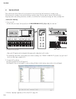

QL5/QL1
132
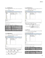
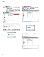
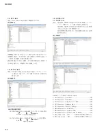
1-6. DSP6 test
1-7. DSP7 test
Contents Checks the condition of the address bus line and data
bus line by writing/reading each register of DSP6/
DSP7.
Compares and checks DSP6 and DSP7 by writing /
reading to DRAM and SDRAM of each DSP6 and
DSP7 through registers.
Checks the SIO connection between DSPs (including
SHARC) by transmitting and receiving signals.
Example of executing screen
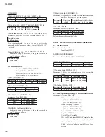
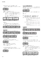
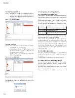
DSP6 test items and display provided during execution.
1: CPU Interface (Data Bus) .................................................OK
2: CPU Interface (Data Bus) .................................................OK
3: CPU Interface (Chip Select, TXB)....................................OK
4: CPU Interface (Address Bus) ............................................OK
5: CPU Interface (BUS W/R Reg.) .......................................OK
6: DRAM Interface (Data Bus) .............................................OK
7: DRAM Interface (Address Bus) .......................................OK
8: DRAM Interface (Address Bus & MPR) ..........................OK
9: SIO Connection.....OK .......................DSP6
→
DSP6 SIO test
A: PIO Connection.....OK .......................DSP6
→
DSP6 SIO test
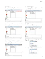
1-4. RTC test
Contents Obtains and sets Real Time Clock.
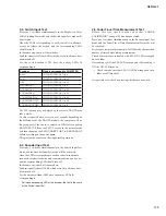
Example of executing screen
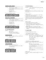
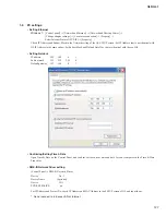
The automatic check (AUTO) is executed. First, sets the
time preset in PC, waits for 1 seconds and judges OK if the
difference with the obtained time is within 1 to 3 seconds.
If it is not possible to set or obtain the time, or the time
difference is below 1 second or more than 3 seconds, judgment
is NG.
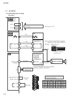
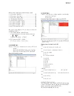
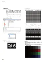
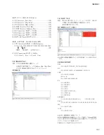
1-5. PLLPU test
Contents Checks the condition of the address bus line
(A0....A4) and data bus line (D0....D15) by writing/
reading the register of PLLPU.
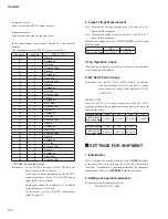
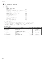
Example of executing screen
Display in case the check result is NG
NG: ADD [080A:5555] → [080A:FFFF] ←
When address bus is NG
NG: DATA [080A:0001] → [080A:FFFF] ←
When data bus is NG
Address bus which is judged as NG.
Data bus which is judged as NG.
write data
read data
write data
read data
Содержание QL5
Страница 1: ...101 QL5 QL1 JK Circuit Board to DSP32 CN751 QL5 to DSP16 CN751 QL1 Component side 2NA WY63490 1...
Страница 3: ...103 QL5 QL1 PNL PNCOM Circuit Board 2NA ZF60470 1 WR 31 0 1 Component side Pattern side...
Страница 4: ...QL5 QL1 104 2NA ZF60450 1 PN16M Circuit Board PN16S Circuit Board QL5 F F...
Страница 5: ...105 QL5 QL1 Component side 2NA ZF60450 1 Scale 90 100 F F...
Страница 8: ...QL5 QL1 108 PNR PNCOM Circuit Board 2NA ZF60470 1 Component side...
Страница 9: ...109 QL5 QL1 PNR PNCOM Circuit Board 2NA ZF60470 1 WR 31 0 1 WR 31 0 1 Pattern side...
Страница 10: ...QL5 QL1 110 FD1M FDCOM Circuit Board FD2 FDCOM Circuit Board QL5 FD1M FD2 2NA ZK68030 H H...
Страница 11: ...111 QL5 QL1 FD1M FD2 2NA ZK68030 H H Component side Scale 90 100...
Страница 13: ...113 QL5 QL1 Pattern side Scale 90 100 not installed I I FD1M FD2 2NA ZK68030...
Страница 14: ...QL5 QL1 114 Pattern side Component side FD1S FDCOM Circuit Board WR 6 1 2NA ZK68030...
Страница 50: ...QL5 QL1 150 2 H 3 O X O 4 BOX 5x4 1 18 LCD Test LCD LCD 1 3 2 9 5 OK NG 1...
Страница 69: ...QL5 QL1 169 5 Start QL OK Status Updating 1 1 6 OK Status Update Done 7 Status Error QL...
Страница 73: ...QL5 QL1 173 CD CD Ctrl Audio CD wav OK 01 01 Ctrl P 8 8 8 8 m ON ON OVER 10 00 dB 0 00 dB...
Страница 89: ...QL5 QL1 189 q w NG OK...
Страница 91: ...QL5 QL1 191 y u i o F1 F12 0 Port Setting error Ethernet Network...
Страница 100: ...QL5 QL1 9 20 20a 20c 20g 20b 20b 20d 20f 20e REAR L ASSEMBLY L Ass y JK SHEET ASSEMBLY JK Ass y 470 470a 470b Solder...