DA824
27
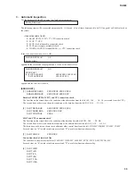
(5) Cross talk between odd channels and even channels
Conditions: Input signal into odd channels.
Even channels shorted using 150 ohms.
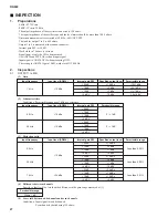
INSPECTION
1.
Preparations
· 0 dBu=0.775 Vrms
· 0 dBV-1 Vrms=2.2 dBu
· The output impedance of the oscillator connected is 150 ohms.
· The input impedance of the oscilloscope and the level meter should be more than 100 k ohms.
· Distortion measurement is corrected at 80 kHz, -6 dB/OCT LPF.
· The load for output 1 to 8 is 600 ohms.
· Output 1 to 8 is measured at the cannon connector.
· Internal gain SW is +18 dB.
· Work clock in 75 ohms is set to on.
· Signal input of only the CH to be measured.
· Use AD824 and MY8-AE card and input signal.
· Input signal to AD824 NCH when measuring NCH.
· The setting for AD824 is gain 10 dB, word clock INT 48 kHz.
2.
Inspections
2-1
OUTPUT1 to 8CH
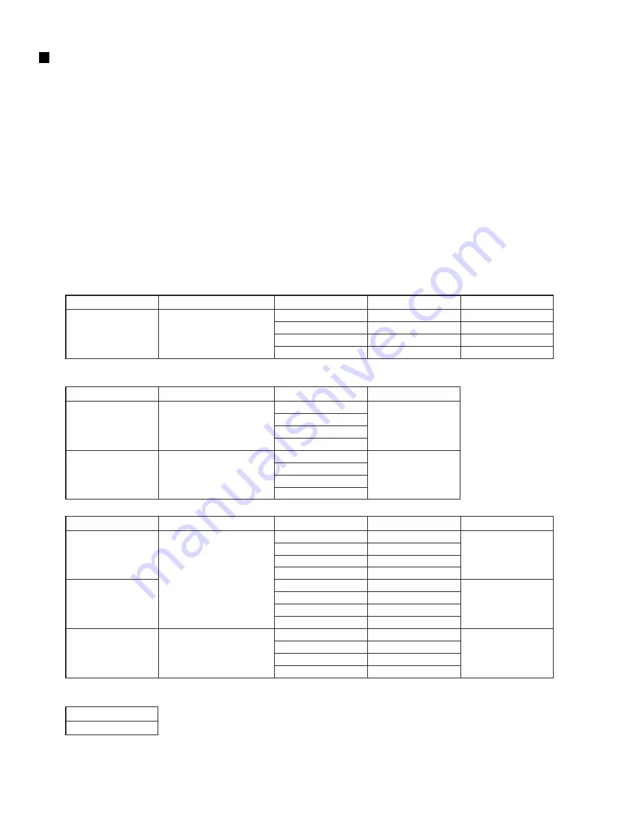
(1) Gain
Input frequency
Input level (AD824)
Internal gain SW
Specified output level
Permissible range
1 kHz
+10 dBu
+24 dB
+18 dB
+15 dB
+4 dBV
+10 dBu
+4 dBu
+1 dBu
-10 dBV
+10
±
1 dBu
+4
±
1 dBu
+1
±
1 dBu
-10
±
1 dBV
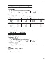
(2) f characteristics
Conditions: Permissible range uses 1 kHz as a reference.
Input frequency
Input level (AD824)
Internal gain SW
Permissible range
20 Hz
20 kHz
+10 dBu
+10 dBu
+24 dB
+18 dB
+15 dB
+4 dBV
+24 dB
+18 dB
+15 dB
+4 dBV
-3 – +1 dB
-3 – +1 dB
(3) Distortion ratio
Input frequency
Input level (AD824)
Internal gain SW
Specified output level
Permissible range
20 Hz
20 kHz
1 kHz
+10 dBu
+24 dBu
+24 dB
+18 dB
+15 dB
+4 dBV
+24 dB
+18 dB
+15 dB
+4 dBV
+24 dB
+18 dB
+15 dB
+4 dBV
+10 dBu
+4 dBu
+1 dBu
-10 dBV
+10 dBu
+4 dBu
+1 dBu
-10 dBV
+24 dBu
+18 dBu
+15 dBu
+4 dBV
Less than 0.05 %
Less than 0.05 %
Less than 0.01 %
(4) Difference between channels
Specify so that it will be less than the difference in the gain range measured at (1).
Permissible range
Within 1 dB
Содержание DA824
Страница 6: ...DA824 6 DIMENTIONS 67 5 67 5 345 430 13 88 H 97 5 2 30 2 30 48 33 274 355 D 366 8 W 480 Unit mm ...
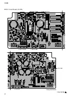
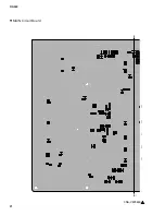
Страница 21: ...E E 3NA V485480 1 DA824 21 MAIN Circuit Board ...
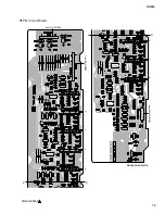
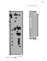
Страница 22: ...E E MAIN MYSL 3NA V485480 1 MYSL Circuit Board Pattern side Pattern side DA824 22 ...
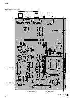
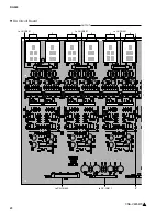
Страница 25: ...3NA V485470 1 G G DA Circuit Board DA824 25 ...
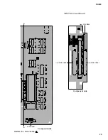
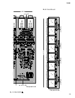
Страница 26: ...DA JK 3NA V485470 1 G G JK Circuit Board Pattern side Pattern side DA824 26 ...


