CDX-497/CDX-397
16
–
–
To be fixed at “H” or “L” when com-
munication is not in progress, so
that the pin will not become HiZ.
To be fixed at “H” when communi-
cation is not in progress, so that
the pin will not become HiZ.
To be connected to 0.1 uF.
–
–
–
Genelal-purpose I/O (input after a
reset).
The playback speed mode flag
output can be switched, using
command bits.
–
–
–
–
–
General-purpose I/O (input after a
reset).
As per CP-1201
–
Normal speed: 32fs = 1.4112 MHz
Normal speed: 44.1kHz
1-bit DAC external input
Controllable in CLV/CAV.
–
Quaternary output (PVDD3, HiZ,
VSS, and PVREF).
Ternary output (PVDD3, VSS, and
Hiz).
34
35
36
37
38
39
40
41
42
43
44
45
46
47
48
49
50
51
52
53
54
55
56
57
58
59
60
61
62
63
64
65
66
67
68
69
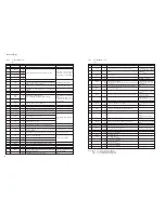
VDDM
VSS1
BUS0
BUS1
BUS2
BUS3
BUCK
/CCE
/RST
STBY
VDDT
FGIN
IO0A
(/HSO)
IO1A
(/UHSO)
TESTD
VSSP
VCOI
VDDP
TESTC
PIO0
PIO1
PIO2
PIO3
DOUT
AOUT
BCK
LRCK
AIN
BCKI
LRCKI
VDD1
VSS1
AWRC
PVDD3
PDO
TMAX
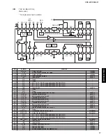
1.5V supply voltage pin dedicated to the DSP/1Mbit SRAM
circuit.
1.5V groundind pin dedicated to the DSP/1Mbit SRAM circuit.
Data input/output pin for the microcontroller interface.
Clock input pin for the microcontroller interface.
Chip enable signal input pin for the microcontroller interface.
BUS3 to BUS0 are active if this pin is “L”.
Reset signal input pin. The internal registers and servo section
registers are reset, respectively, when the reset signal is “L”
and on the positive-going edge of the reset signal.
STANDBY control pin dedicated to the DSP/1Mbit SRAM
circuit.
3.3V supply voltage pin dedicated to the Digital I/O circuit.
FG signal input pin for CAV.
CLV: “L”. CAV: FG input.
Genelal-purpose input/output pins.
(Pin for outputting the playback speed mode flag.)
DSP/Test input pin. Usually fixed at “L”.
1.5V grounding pin dedicated to the DSP/VCO circuit.
PD output pin dedicated to the DSP/VCO circuit.
1.5V supply voltage pin dedicated to the DSP/VCO circuit.
CD/Test input pin. Usually fixed at “L”.
General-purpose I/O (CD/DSP)
General-purpose I/O (CD/DSP)
General-purpose I/O (DSP)
General-purpose I/O (DSP)
Digital-out output pin. Digital data for up to double speed can
be output when a frequency of 16.9344 MHz is used.
Audio data output pin. Which bit is first (MSB first or LSB first)
can be selected, using a command.
Bit clock output pin. 32fs, 48fs, and 64fs can be selected,
using a command.
LR channel clock output pin. L for the L-channel and “H” for
the R-channel. The output polarity can be inverted, using a
command.
1-bit DAC external input: AIN
1-bit DAC external input: BCKI
1-bit DAC external input: LRCKI
1.5V supply voltage pin dedicated to the DSP circuit.
1.5V grounding pin dedicated to the DSP circuit.
VCO control pin for active wide range.
3.3V supply voltage pin dedicated to the PLL circuit.
Pin for outputting a phase difference signal between the EFM
signal and PLCK signal.
Pin for outputting the result of TMAX detection.
The TMAX pin output the same signal.
–
–
I/O
3I/F
I/O
3I/F
I/O
3I/F
I/O
3I/F
I
3I/F
I
3I/F
I
3I/F
I
3I/F
–
I
3AI/F
I/O
3I/F
I/O
3I/F
I
3I/F
–
O
1.5AI/F
–
I
3I/F
I/O
3I/F
I/O
3I/F
I/O
3I/F
I/O
3I/F
O
3I/F
O
3I/F
O
3I/F
O
3I/F
I
3I/F
I
3I/F
I
3I/F
–
–
O
3AI/F
–
O
3AI/F
O
3AI/F
Remark
IC21
: TC94A54 (MAIN P.C.B)
DSP
Pin No.
Pin name
Function
Pin name
70
71
72
73
74
75
76
77
78
79
80
81
82
83
84
85
86
87
88
89
90
91
92
93
94
95
96
97
98
99
100
LPFN
LPFO
PVREF
VCOF
VCOREF
PVSS3
SLCO
RFI
RFRPI
RFEQO
RESIN
VRO
VMDIR
TESTR
INVSEL
AGCI
AGCI
RFO
PNSEL
EQSET
RVDD3
LDO
MDI
RVSS3
FNI2
FNI1
FPI2
FPI1
TPI
TNI
FTE
I
3AI/F
O
3AI/F
–
O
3AI/F
I
3AI/F
–
O
3AI/F
I
3AI/F
I
3AI/F
O
3AI/F
I
3AI/F
O
3AI/F
–
O
3AI/F
I
3AI/F
I
3AI/F
I
3AI/F
O
3AI/F
I
3AI/F
O
3AI/F
–
O
3AI/F
I
3AI/F
–
I
3AI/F
I
3AI/F
I
3AI/F
I
3AI/F
I
3AI/F
I
3AI/F
O
3AI/F
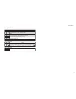
Pin for receiving an inverted output of the PLL-circuit low-pass
filter amp.
Pin for the PLL-circuit low-pass filter amp output.
1.65V reference supply voltage pin dedicated to the PLL
circuit.
VCO filter pin.
Input pin for the VCO center frequency reference level.
3.3V grounding pin dedicated to the PLL circit.
EFM slice level output pin.
For both analog and digital slice modes, the output impedance
= 2.5 k-ohms.
RF signal input pin.
The input resistance can be selected, using a command.
RF ripple signal input pin.
RF equalizer circuit output pin.
Pin for connecting a reference current generating resistance.
1.65V reference voltage output pin.
Reference voltage poutput pin for the APC circuit.
LPF pin for RFEQO offset correction.
Test pin, usually fixed at “L”.
Pin for RF signal amplitude adjustment amp input.
RF signal peak detsction input pin.
RF signal generation amp output pin.
Test pin, usually fixed at “H”.
External connection pin for the RF signal equalizer.
3.3V supply voltage pin for the Rfamp core section.
Laser diode amp output pin.
Monitor photodiode amp input pin.
3.3V grounding pin for the RF amp core section.
Main beam input pin.
Connected to PIN diode C.
Main beam input pin.
Connected to PIN diode A.
Main beam input pin.
Connected to PIN diode D.
Main beam input pin.
Connected to PIN diode B.
Subbeam input pin.
Connected to PIN diode F.
Subbeam input pin.
Connected to PIN diode E.
Focus /tracking signal output.
(Test pin for servo characteristic measurement.)
The resistance side is connected.
See an applicable circuit diagram.
The capacitor side is connected.
See an spplicable circuit diagram.
Connected to the VREF and PVREF
within the IC.
A 0.1 uF capacitor is connected.
–
To be connected to the PVREF if
the AWRC is not used.
–
A capacitor to be connected is se-
lected according to the servo op-
eration band.
Zin: 20 k-ohms, 10 k-ohms, 5 k-
ohms
–
To be connected to the RFRPI via
0.1 uF and to the RFI via 4700 pF
or higher.
To be connected to 22 k-ohms
and 680 pF in parallel.
Connected to the VREF and
PVREF within the IC
To be connected to 0.1uF anf 100
uF.
To be connected to 0.1uF.
To be connected to 0.015 uF or
higher.
–
–
–
To be connected directly to the
RFDCI.
To ne connected to the AGCI via
0.1 uF.
To be kept open when the RFEQ
is used.
–
Reference to 178 mV (typ.)
–
–
–
–
–
–
–
Switchable using a command.
I/O
Pin No.
Pin name
Description
Remark
Note: “3AI/F
: 3V circuit analog input/output pin.”
“3I/F
: 3V circuit digital input/output pin.”
“1.5AI/F : 1.5V circuit analog input/output pin.”
IC21
: TC94A54 (MAIN P.C.B)
DSP
Содержание CDX-497
Страница 4: ...CDX 497 CDX 397 4 CDX 497 CDX 397 ...
Страница 27: ...CDX 497 CDX 397 27 MEMO MEMO MEMO MEMO ...

