


Alignment
ALIGNMENT-12
FT-99
1
Technical Supplement
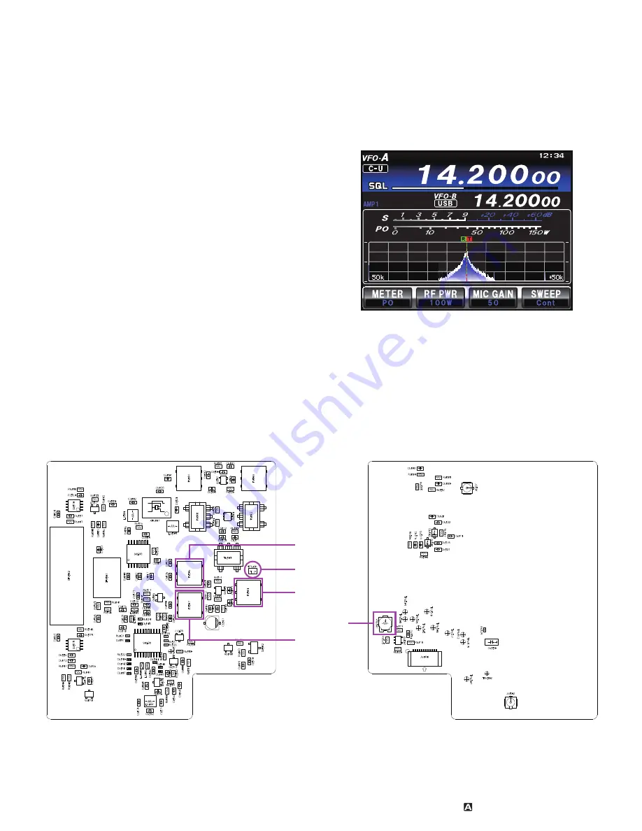
Scope Adjustment
Set the VFO-A frequency to 14.200 MHz in the
CW mode.
Set the following controls as indicated:
[IPO] : AMP1
[ATT] : OFF
[AGC] : AUTO
[RF GAIN] : Fully clockwise
Connect the RF Signal Generator to the “HF/50
MHz” ANT jack, then set the frequency to
14.200 MHz.
Connect the RF millivoltmeter to TP6501 on the
SCP Unit.
Adjust T6507, T6506 and T6504 on the SCP
Unit in succession several times for maximum
deflection on the RF millivoltmeter.
Set the RF Signal Generator output level to +36
dBµ at the 14.200 MHz.
Press the assigned [A], [B] or [C] key to activate
the SCOPE function.
T6506
TP6501
T6504
T6507
VR6501
Adjust T6501 on the SCP Unit for maximum
deflection on the SCOPE display.
Turn the RF Signal Generator OFF.
As shown in the figure below, adjust VR6501 so
the waveform matches the second line from the
top on the scope display.
Содержание FT-991A
Страница 10: ...BLOCK DIAGRAM 1 FT 991 Technical Supplement Block Diagram...
Страница 11: ...CONNECTION DIAGRAM 1 FT 991 Technical Supplement Connection Diagram...
Страница 36: ...FT 991 Technical Supplement MAIN 1 Circuit Diagram MAIN Unit...
Страница 37: ...FT 991 Technical Supplement MAIN 2 Parts Layout side A MAIN Unit 1 2 3 4 5 A B C D E F G...
Страница 38: ...FT 991 Technical Supplement MAIN 3 Parts Layout side B MAIN Unit 1 2 3 4 5 a b c d e f g...
Страница 68: ...FT 991 Technical Supplement PLL 1 PLL Unit Circuit Diagram...
Страница 69: ...FT 991 Technical Supplement PLL 2 PLL Unit Parts Layout side A side B 1 2 3 A B C...
Страница 73: ...FT 991 Technical Supplement EDSP 1 Circuit Diagram EDSP Unit...
Страница 74: ...FT 991 Technical Supplement EDSP 2 Parts Layout EDSP Unit side A side B 1 2 3 A B C D 1 2 3 a b c d 4 4...
Страница 79: ...FT 991 Technical Supplement CNTL 1 CNTL Unit Circuit Diagram...
Страница 80: ...FT 991 Technical Supplement CNTL 2 CNTL Unit Parts Layout side A A B C D E F G 1 2 3 4...
Страница 81: ...FT 991 Technical Supplement CNTL 3 CNTL Unit Parts Layout side B a b c d e f g 1 2 3 4...
Страница 87: ...FT 991 Technical Supplement HF PA 1 HF PA Unit Circuit Diagram...
Страница 88: ...FT 991 Technical Supplement HF PA 2 HF PA Unit Parts Layout side A 1 2 3 4 A B D F G E C 5...
Страница 89: ...FT 991 Technical Supplement HF PA 3 HF PA Unit Parts Layout side B 1 2 3 4 a b d f g e c 5...
Страница 96: ...FT 991 Technical Supplement V_U PA 1 Circuit Diagram V_U PA Unit...
Страница 97: ...FT 991 Technical Supplement V_U PA 2 V_U PA Unit Parts Layout side A 1 2 3 A B C D E F G H...
Страница 98: ...FT 991 Technical Supplement V_U PA 3 V_U PA Unit Parts Layout side B 1 2 3 a b c f h j d e g i...
Страница 105: ...FT 991 Technical Supplement PANEL 1 Circuit Diagram PANEL Unit...
Страница 106: ...FT 991 Technical Supplement PANEL 2 Parts Layout PANEL Unit side A side B 1 2 3 a b c d e f g h A B C D E F G H 1 2 3...
Страница 113: ...FT 991 Technical Supplement TUNER 1 TUNER Unit Circuit Diagram...
Страница 114: ...FT 991 Technical Supplement TUNER 2 TUNER Unit Parts Layout side A 1 2 3 4 A B C D E F G H...
Страница 115: ...FT 991 Technical Supplement TUNER 3 TUNER Unit Parts Layout side B...
Страница 119: ...JACK 1 JACK Unit Circuit Diagram FT 991 Technical Supplement...
Страница 120: ...JACK 2 JACK Unit Parts Layout side A side B FT 991 Technical Supplement...
Страница 122: ...FT 991 Technical Supplement SCP 1 Circuit Diagram SCP Unit...
Страница 123: ...FT 991 Technical Supplement SCP 2 Parts Layout SCP Unit side A side B...
Страница 127: ...FT 991 Technical Supplement DSP 1 DSP Unit Circuit Diagram...
Страница 128: ...FT 991 Technical Supplement DSP 2 DSP Unit Parts Layout side A side B...