


ZC706 Evaluation Board User Guide
29
UG954 (v1.5) September 10, 2015
Feature Descriptions
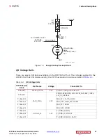
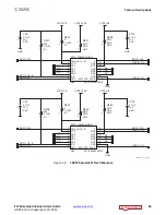
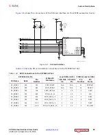
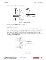
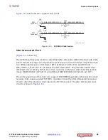
shows the USB 2.0 ULPI transceiver circuitry. Note that the shield for the USB
Micro-B connector (J2) can be tied to GND by a jumper on header J51 pins 1–2 (default).
The USB shield can optionally be connected through a capacitor to GND by installing a
capacitor (body size 0402) at location C335 and jumping pins 2-3 on header J51.
SD Card Interface
[
, callout 5]
The ZC706 evaluation board includes a secure digital input/output (SDIO) interface to
provide user-logic access to general purpose nonvolatile SDIO memory cards and
peripherals. Information for the SD I/O card specification can be found at the SanDisk and
SD card websites
.
The SDIO signals are connected to XC7Z045 AP SoC PS bank 501 which has its VCCMIO set
to 1.8V. A MAX13035E high-speed logic-level translator (U11) is used between XC7Z045 AP
SoC 1.8V PS bank 501 and the 3.3V SD card connector (J30).
X-Ref Target - Figure 1-7
Figure 1-7:
USB 2.0 ULPI Transceiver
EN
OUT2
IN
GND
NC1
FLG
NC2
OUT1
REFSEL2_14
DATA0_3
RBIAS_23
ID_23
VBUS_22
VBAT_21
VDD33_P
DM_19
DP_18
CPEN33_17
NC_12
REFSEL0_8
DATA4_7
DATA6_10
CLKOUT_1
NXT_2
DATA2_5
REFSEL1_11
VDDIO_32
DIR_31
DATA5_9
DATA7_13
DATA1_4
SPK_L_15
R
EFCLK_26
SPK_R_16
XO_25
VDD18_30
DATA3_6
STP_29
VDD18_28
RESETB_27
CTR_GND_33
SHLD5
SHLD6
GND
SHLD4
VBUS
D_N
D_P
SHLD1
SHLD2
SHLD3
ID
1-2 = DEVICE MODE
OFF = DEVICE MODE
2-3 = HOST OR OTG MODE
ON = HOST OR OTG MODE
USB HOST POWER
1-2 = A/B CABLE DETECT
2-3 = ID NOT USED
3 PLACES
2 PLACES
CVBUS Select:
1-2: OTG Mode
2-3: Host Mode
1
2
L11
FERRITE-220
USB_D_P
27
USB_D_N
27
USB_RESET_B
31
USB_STP
9
USB_DIR
9
USB_DATA7
8
USB_DATA6
8
USB_DATA5
8
USB_DATA4
8
1
2
C76
0.1UF
25V
31
USB_D_N
2
1
R267
10.0K
1/10W
GND
1
2
J10
1
2
C380
1UF
16V
X5R
10 11
5
9
1
2
3
6 7 8
4
J2
ZX62D_AB_5P8
GND
GND
1
2
C484
120UF
20V
TANT
3
2
1
J50
GND
1
2
3
J49
USB_CLKOUT
8
USB_NXT
8
USB_DATA1
8
USB_DATA0
8
USB_DATA2
8
USB_DATA3
8
14
3
24
23
22
21
20
19
18
17
12
8
7
10
1
2
5
11
32
31
9
13
4
15
26
16
25
30
6
29
28
27
33
U12
USB3320_QFN32
USB3320_QFN32
GND
1
2
C71
1
2
C70
0.1UF
25V
2
1
C496
18PF
50V
NPO
GND
GND
2
1
X2
24.000MHZ
GND
2
1
C209
2.2UF
6.3V
GND
GND
VCC5V0
GND
2
1
C335
DNP
1
2
3
J48
USB_VBUS_SEL
VCC5V0
2
1
C447
5.6UF
10V
1
2
L12
FERRITE-220
VCC3V3
GND
2
1
DS25
LED-RED-SMT
2
1
R389
261
1/10W
1
8
7
3
4
2
5
6
U22
SOP127P500X600_8
MIC2025_SOP8
2
1
R359
1.00K
1/16W
GND
1
2
C75
0.1UF
25V
USB_VBUS_SEL
1
2
3
J51
1
2
C469
150UF
10V
TANT
GND
2
1
C497
18PF
50V
NPO
2
1
R403
1.0M
1/10W
5%
1
2
C74
USB_ID
27
USB_VDD33
27
USB_ID
31
USB_D_P
31
NC
NC
NC
NC
NC
USB_VDD33
27
GND
2
1
R178
8.06K 1/10W 1%
2
1
25V
0.1UF
C72
VCCMIO
VCCP1V8
UG954_c1_07_041113


