Virtex-6 FPGA System Monitor
17
UG370 (v1.1) June 14, 2010
Register File Interface
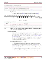
Flag Register
The Flag Register is shown in
. The bit definitions are described in
Control Registers
The System Monitor control registers (
) are located at addresses
40h
to
7Fh
. These
registers are used to configure the System Monitor operation. System Monitor
functionality (ADC operating modes, Channel Sequencer, and Alarm limits) is controlled
through these registers. System Monitor functionality is explained in
.
The control registers are initialized using the SYSMON attributes when System Monitor is
instantiated in a design. This means that System Monitor can be configured to start in a
predefined mode after FPGA configuration.
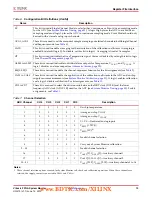
Configuration Registers (
40h
to
42h
)
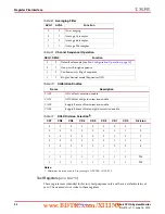
The first three registers in the control register block are used to configure the System
Monitor operating modes. These registers are known as System Monitor configuration
registers. The configuration registers bit definitions are illustrated in
. The
X
s in
define these bit positions as
don’t cares
. Bits 0, 1, and 2 in configuration register 2
(
42h
) should
always
be set to 0.
The configuration registers are modifiable through the DRP after the FPGA has been
configured. For example, a soft microprocessor or state machine can be used to alter the
contents of the System Monitor control registers at any time during normal operation.
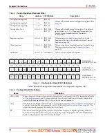
Undefined
27h
to
3Eh
These locations are unused and contain invalid data.
Flag
3Fh
This register contains general status information - see
Table 3:
Status Registers (Read-Only)
(Cont’d)
Name
Address
Description
X-Ref Target - Figure 8
Figure 8:
Flag Register
Table 4:
Flag Register Definitions
Name
Description
OT
This bit reflects the status of the Over Temperature logic output
DIS
When this bit is a logic
1
, the System Monitor is disabled by connecting the supplies and reference
inputs to AGND.
REF
When this bit is a logic
1
, the System Monitor ADC is using the internal voltage reference. When it is
a logic
0
, then the external reference is being used.
Flag Register
DADDR [6:0] = 3Fh
DI0
DI1
DI2
DI3
DI4
DI5
DI6
DI7
DI8
DI9
DI10
DI11
DI12
DI13
DI14
DI15
X
OT
DIS
X
X
X
X
X
X
X
X
REF
X
X
X
X
UG370_08_060709
www.BDTIC.com/XILINX


