VC707 Evaluation Board
7
UG885 (v1.2) February 1, 2013
Feature Descriptions
•
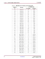
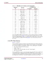
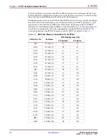
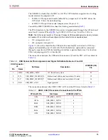
Linear BPI Flash memory
•
USB JTAG configuration port
•
Platform cable header JTAG configuration port
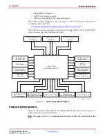
The VC707 board block diagram is shown in
. The VC707 board schematics are
available for download from:
www.xilinx.com/products/boards-and-kits/EK-V7-VC707-G.htm
The VC707 board can be damaged by electrostatic discharge (ESD). Follow standard ESD
prevention measures when handling the board
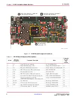
Feature Descriptions
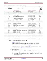
shows the VC707 board. Each numbered feature that is referenced in
is described in the sections that follow.
Note:
is for reference only and might not reflect the current revision of the
board.
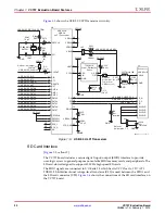
X-Ref Target - Figure 1-1
Figure 1-1:
VC707 Board Block Diagram
UG885_c1_01_030512
Virtex-7 FPGA
XC7VX485T-2FFG1761C
128 MB Linear BPI
Flash memory
USB 2.0
ULPI PHY
8-lane PCI Express
Edge Connector
LCD Display
(2 line x 16 characters)
1 KB EEPROM (I2C)
I2C Bus Switch
XADC Header
User Switches,
Buttons, and LEDs
HDMI Video
Interface
Differential Clock
GTX SMA Clock
1 GB DDR3 Memory
(SODIMM)
FMC Connectors
(HPC/HPC)
10/100/1000 Ethernet
Interface
DIP Switch SW11
Config and Flash Addr
USB-to-UART Bridge
JTAG Interface
mini-B USB Connector
SFP+ Single Cage
Содержание VC707
Страница 1: ...VC707 Evaluation Board for the Virtex 7 FPGA User Guide UG885 v1 2 February 1 2013...
Страница 74: ...74 www xilinx com VC707 Evaluation Board UG885 v1 2 February 1 2013 Chapter 1 VC707 Evaluation Board Features...
Страница 94: ...94 www xilinx com VC707 Evaluation Board UG885 v1 2 February 1 2013 Appendix D Board Setup...
Страница 96: ...96 www xilinx com VC707 Evaluation Board UG885 v1 2 February 1 2013 Appendix E Board Specifications...

