16
VC707 Evaluation Board
UG885 (v1.2) February 1, 2013
Chapter 1:
VC707 Evaluation Board Features
80 MHz oscillator connected to the FPGA's EMCCLK pin with a bitstream that has been
built to divide the configuration clock by two. The division is necessary to remain within
the synchronous read timing specifications of the flash memory.
Multiple bitstreams can be stored in the Linear BPI Flash. The two most significant address
bits (A25, A24) of the flash memory are connected to DIP switch SW11 positions 1 and 2
respectively, and to the RS1 and RS0 pins of the FPGA. By placing valid XC7VX485T
bitstreams at four different offset addresses in the flash memory, 1 of the 4 bitstreams can
be selected to configure the FPGA by appropriately setting the DIP switch SW11. The
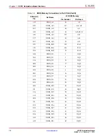
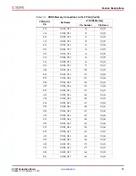
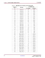
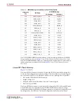
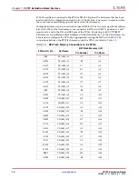
connections between the BPI Flash memory and the FPGA are listed in
.
Table 1-5:
BPI Flash Memory Connections to the FPGA
FPGA (U1) Pin
Net Name
BPI Flash Memory (U3)
Pin Number
Pin Name
AJ28
FLASH_A0
A1
A1
AH28
FLASH_A1
B1
A2
AG31
FLASH_A2
C1
A3
AF30
FLASH_A3
D1
A4
AK29
FLASH_A4
D2
A5
AK28
FLASH_A5
A2
A6
AG29
FLASH_A6
C2
A7
AK30
FLASH_A7
A3
A8
AJ30
FLASH_A8
B3
A9
AH30
FLASH_A9
C3
A10
AH29
FLASH_A10
D3
A11
AL30
FLASH_A11
C4
A12
AL29
FLASH_A12
A5
A13
AN33
FLASH_A13
B5
A14
AM33
FLASH_A14
C5
A15
AM32
FLASH_A15
D7
A16
AV41
FLASH_A16
D8
A17
AU41
FLASH_A17
A7
A18
BA42
FLASH_A18
B7
A19
AU42
FLASH_A19
C7
A20
AT41
FLASH_A20
C8
A21
BA39
FLASH_A21
A8
A22
BA39
FLASH_A22
G1
A23
BB39
FLASH_A23
H8
A24
AW42
FLASH_A24
B6
A25
Содержание VC707
Страница 1: ...VC707 Evaluation Board for the Virtex 7 FPGA User Guide UG885 v1 2 February 1 2013...
Страница 74: ...74 www xilinx com VC707 Evaluation Board UG885 v1 2 February 1 2013 Chapter 1 VC707 Evaluation Board Features...
Страница 94: ...94 www xilinx com VC707 Evaluation Board UG885 v1 2 February 1 2013 Appendix D Board Setup...
Страница 96: ...96 www xilinx com VC707 Evaluation Board UG885 v1 2 February 1 2013 Appendix E Board Specifications...


