


116
RocketIO™ Transceiver User Guide
UG024 (v3.0) February 22, 2007
Chapter 3:
Analog Design Considerations
R
routing of high-speed serial traces should be on signal layers that share a reference plane.
If the signal layers do not share a reference plane, a capacitor of value 0.01
μ
F should be
connected across the two reference layers close to the vias where the signals change layers.
If both of the reference layers are DC coupled (if they are both ground), they can be
connected with vias close to where the signals change layers.
To control crosstalk, serial differential traces should be spaced at least five trace separation
widths from all other PCB routes, including other serial pairs. A larger spacing is required
if the other PCB routes carry especially noisy signals, such as TTL and other similarly noisy
standards.
The RocketIO transceiver is designed to function at 3.125 Gb/s through 40 inches of PCB
with two high-bandwidth connectors. Longer trace lengths require either a low-loss
dielectric or considerably wider serial traces.
Differential Trace Design
The characteristic impedance of a pair of differential traces depends not only on the
individual trace dimensions, but also on the spacing between them. The RocketIO
transceivers require either a 100
Ω
or 150
Ω
differential trace impedance (depending on
whether the 50
Ω
or 75
Ω
termination option is selected). To achieve this differential
impedance requirement, the characteristic impedance of each individual trace must be
slightly higher than half of the target differential impedance. A field solver should be used
to determine the exact trace geometry suited to the specific application (
). This
task should not be left up to the PCB vendor.
Trace lengths up to 20" in FR4 may be of any width, provided that the differential
impedance is 100
Ω
or 150
Ω
. Trace lengths between 20" and 40" in FR4 must be at least
8 mils wide and have a differential impedance of 100
Ω
or 150
Ω
. For information on other
dielectric materials, please contact your Xilinx representative or the Xilinx Hotline.
Differential impedance of traces on the finished PCB should be verified with Time Domain
Reflectometry (TDR) measurements.
Tight coupling of differential traces is recommended. Tightly coupled traces (as opposed to
loosely coupled) maintain a very close proximity to one another along their full length.
Since the differential impedance of tightly coupled traces depends heavily on their
proximity to each other, it is imperative that they maintain constant spacing along their full
length, without deviation. If it is necessary to separate the traces in order to route through
a pin field or other PCB obstacle, it can be helpful to modify the trace geometry in the
vicinity of the obstacle to correct for the impedance discontinuity (increase the individual
trace width where trace separation occurs).
show examples of
PCB geometries that result in 100
Ω
differential impedance.
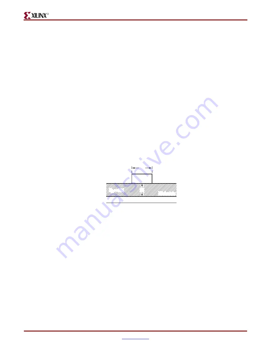
Figure 3-12:
Single-Ended Trace Geometry
UG024_21_042903
Trace
Reference Plane
Dielectric
W
H
W = 7.9 mil (0.201 mm)
H = 5.0 mil (0.127 mm)
Z
0
= 50
Ω
E
r
= 4.3
Product Not Recommended for New Designs