FPGA Design Demonstration Board
Hardware User Guide
3-23
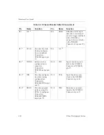
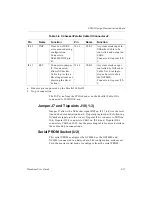
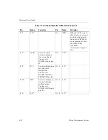
Jumper J5 allows the XChecker Cable signal RST on J1-17 to drive the
reset line on the demonstration board. Tiepoint pins jumper the
following XChecker Cable signals into your circuit. Tiepoint J3-1
connects to TRIG on J1-6; Tiepoint J3-2 connects to CLK1 on J1-16;
and, Tiepoint J3-3 connects to CLK0 on J1-18. See the preceding table
for more information on cable connections.
Serial PROM Socket (U1)
This serial PROM configures the XC3020A. You must use the master
serial mode to configure from the serial PROM.
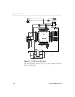
Relaxation Oscillator Components (R1 C5, R2 C6)
R1, C5 and R2, C6 are two RC networks that connect to the XC3020A
at pins 12 and 14. These RC networks are for use in a relaxation oscil-
lator such as the circuit is shown in the following figure.
J1–15
N.C.b
J1–16
CLKI
System clock input to
XChecker Cable to be
controlled and output
on CLKO. Connects to
tiepoint J3–2.
J1–17
RST
Connects to jumper
J5. If connected,
allows XChecker
Cable to provide a
Reset input (same as
pressing Reset
button).
J1–18
CLKO
System clock output
controlled by
XChecker Cable; used
to single-step or burst
clocks to the XC3020A.
Connects to tiepoint
J3–3.
a.
Denotes pins supported by the Parallel Cable III
b.
No pin connection
Table 3-7 XChecker/Parallel Cable III Connector J1
Pin
Name
Function
Pin
Name
Function
Содержание MultiLINX DLC4
Страница 2: ...Hardware User Guide ...
Страница 10: ...Hardware User Guide vi Xilinx Development System ...
Страница 38: ...Hardware User Guide 1 24 Xilinx Development System ...
Страница 108: ...Hardware User Guide Glossary 4 Xilinx Development System ...


