FPGA Design Demonstration Board
Hardware User Guide
3-9
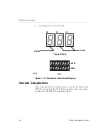
Seven-Segment Displays (U6, U7, U8)
Three seven-segment displays are included with the leftmost display
(U6) connect to the XC3020A FPGA. The rightmost two displays (U7
and U8) connect to the XC4003E device.
Each LED segment is turned on by driving the corresponding FPGA
pin ‘LOW’ with a logic ‘0.’ The decimal point on U8 connects to the
INIT pin of the XC4003E (pin 41) and serves as a programming error
indicator. The decimal point should be on while the FPGA is in its
internal clearing state, then it should remain off during configuration.
If the decimal point comes back on, a programming error has
occurred.
The decimal points on U6 and U7 are tied to the Low During Config-
uration (LDC) pins of the XC3020A and XC4003E, respectively. The
decimal points are on while the FPGAs wait to be configured.
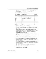
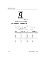
The following table shows the I/O pin definitions. The following
figure shows the seven-segment display of the FPGA demonstration
board.
Table 3-3 Seven-Segment I/O Connections
Display Segment
XC3020A
XC4003E
XC4003E
U6
U7
U8
a
38
39
49
b
39
38
48
c
40
36
47
d
56
35
46
e
49
29
45
f
53
40
50
g
55
44
51
decimal point
30
37
41
Содержание MultiLINX DLC4
Страница 2: ...Hardware User Guide ...
Страница 10: ...Hardware User Guide vi Xilinx Development System ...
Страница 38: ...Hardware User Guide 1 24 Xilinx Development System ...
Страница 108: ...Hardware User Guide Glossary 4 Xilinx Development System ...

