


AXI Bridge for PCI Express v2.4
10
PG055 June 4, 2014
Chapter 2:
Product Specification
Performance
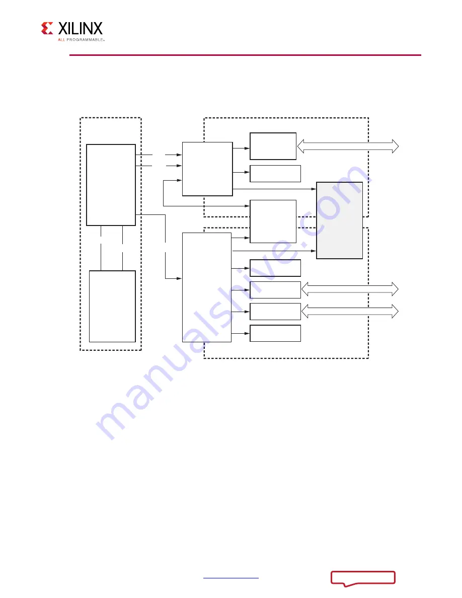
shows a configuration diagram for a target FPGA.
The target FPGA is filled with logic to drive the lookup table (LUT) and block RAM utilization
to approximately 70% and the I/O utilization to approximately 80%.
Maximum Frequencies
The maximum frequency for the AXI clock is 125 MHz for 7 series FPGAs.
Line Rate Support for PCIe Gen1/Gen2
The link speed, number of lanes supported, and support of line rate for PCIe are defined in
. Achieving line rate for PCIe is dependent on the device family, the AXI clock
X-Ref Target - Figure 2-2
Figure 2-2:
FPGA System Configuration Diagram
AXI4-Lite
MicroBlaze
Controller
AXI INTC
AXI GPIO
AXI UARTLite
AXI4
Memory
Controller
MDM
MicroBlaze
Domain
AXI4
Block RAM
Controller
D_LMB
I_LMB
(IC)
AXI Block Ram
(DC)
AXI PCIe
Memory
(DP)
LEDs
RS232
AXI CDMA
MemoryMap
Interconnect
(AXI4)
Control
Interface
Subset
Interconnect
(AXI4-Lite)


