34
KC724 GTX Transceiver Characterization Board
UG932 (v2.2) October 10, 2014
Chapter 1:
KC724 Board Features and Operation
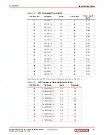
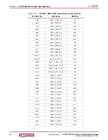
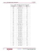
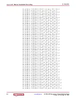
AK6
FMC1_LA26_N
D27
AJ8
FMC1_LA27_P
C26
AK8
FMC1_LA27_N
C27
AK5
FMC1_LA28_P
H31
AK4
FMC1_LA28_N
H32
AA15
FMC1_LA29_P
G30
AB15
FMC1_LA29_N
G31
AC16
FMC1_LA30_P
H34
AC15
FMC1_LA30_N
H35
AC14
FMC1_LA31_P
G33
AD14
FMC1_LA31_N
G34
AA17
FMC1_LA32_P
H37
AA16
FMC1_LA32_N
H38
Y16
FMC1_LA33_P
G36
Y15
FMC1_LA33_N
G37
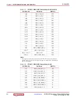
W19
FMC1_PRSNT_M2C_L
H2
U23.8
FMC1_FMC2_TCK
D29
U23.3 / U19.1
FMC1_TDI
D30
U23.6
FMC1_FMC2_TMS
D33
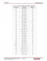
Notes:
1. This signal is not directly connected to the FPGA. The value in the leftmost
column represents the device and pin the signal is connected to. For example,
U39.10 = U39 pin 10.
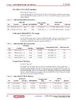
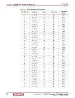
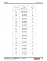
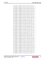
Table 1-18:
VITA 57.1 FMC2 HPC Connections at JA2
U1 FPGA Pin
Net Name
FMC Pin
F12
FMC2_CLK0_M2C_P
H4
E13
FMC2_CLK0_M2C_N
H5
H14
FMC2_CLK1_M2C_P
G2
G14
FMC2_CLK1_M2C_N
G3
K28
FMC2_CLK2_BIDIR_P
K4
K29
FMC2_CLK2_BIDIR_N
K5
M28
FMC2_CLK3_BIDIR_P
J2
L28
FMC2_CLK3_BIDIR_N
J3
AD23
FMC2_HA00_CC_P
F4
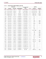
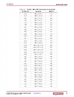
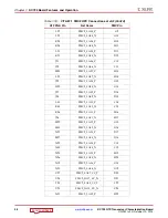
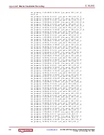
Table 1-17:
VITA 57.1 FMC1 HPC Connections at JA2
(Cont’d)
U1 FPGA Pin
Net Name
FMC Pin

