background image

FMC XM101 User Guide

www.xilinx.com

5

UG538 (v1.1) September 24, 2010

Preface

About This Guide

This document describes the FPGA Mezzanine Card (FMC) XM101 LVDS QSE card, 
referred to as the 

XM101

 in this guide. Xilinx® supported evaluation (carrier) boards are 

referred to simply as 

boards

 in this guide.

Guide Contents

This manual contains the following chapter:

Chapter 1, XM101

.

Additional Documentation

Prior to using the XM101, users should be familiar with Xilinx resources. See the following 
locations for additional documentation on Xilinx tools and solutions:

ISE® Design Suite: 

www.xilinx.com/ise

Answer Browser: 

www.xilinx.com/support

Intellectual Property: 

www.xilinx.com/ipcenter

Information about the latest 

VITA 57 FMC Specification

 is located at:

www.vita.com/fmc.html

The XM101 can be used with Xilinx FMC high pin count (HPC) boards and, with limited 
functionality, FMC low pin count (LPC) boards. Board documentation, schematics and 
PCB design files are available at 

www.xilinx.com/fmc

.

Additional Support Resources

To find additional documentation, see the Xilinx website at:

www.xilinx.com/support/documentation/index.htm

To search the Answer Database of silicon, software, and IP questions and answers, or to 
create a technical support WebCase, see the Xilinx website at:

www.xilinx.com/support/mysupport.htm

Содержание FMC XM101 LVDS QSE

Страница 1: ...FMC XM101 LVDS QSE Card User Guide UG538 v1 1 September 24 2010 ...

Страница 2: ...disclaims any liability in connection with technical support or assistance that may be provided to you in connection with the Information THE DOCUMENTATION IS DISCLOSED TO YOU AS IS WITH NO WARRANTY OF ANY KIND XILINX MAKES NO OTHER WARRANTIES WHETHER EXPRESS IMPLIED OR STATUTORY REGARDING THE DOCUMENTATION INCLUDING ANY WARRANTIES OF MERCHANTABILITY FITNESS FOR A PARTICULAR PURPOSE OR NONINFRINGE...

Страница 3: ...erview 7 Quick Start 7 System Requirements 7 Hardware 7 Software 7 Package Contents 8 Necessary Equipment 8 System Setup 8 Technical Support 9 XM101 Board Technical Description 10 Detailed Description 11 1 VITA 57 1 FMC HPC Connector J1 13 2 Samtec QSE Connectors 13 3 PCA9543 IIC Bus Switch 18 4 Silicon Labs Si570 Clock Sources 20 5 SMA Clock Connections 21 6 M24C02 2 Kb IIC EEPROM 21 Table of Con...

Страница 4: ...4 www xilinx com FMC XM101 User Guide UG538 v1 1 September 24 2010 ...

Страница 5: ...tions ISE Design Suite www xilinx com ise Answer Browser www xilinx com support Intellectual Property www xilinx com ipcenter Information about the latest VITA 57 FMC Specification is located at www vita com fmc html The XM101 can be used with Xilinx FMC high pin count HPC boards and with limited functionality FMC low pin count LPC boards Board documentation schematics and PCB design files are ava...

Страница 6: ...6 www xilinx com FMC XM101 User Guide UG538 v1 1 September 24 2010 Preface About This Guide ...

Страница 7: ... CLK1_M2C_P N SMA J2 J3 SP605 J2 LA 00 33 CLK0_M2C_P N Si570 U1 CLK1_M2C_P N SMA J2 J3 SP601 J1 LA 00 33 CLK0_M2C_P N Si570 U1 CLK1_M2C_P N SMA J2 J3 Software Example designs that use this hardware are not provided Table 1 1 FMC Supported Boards Xilinx Platform Part Number FMC HPC Connector FMC LPC Connector Virtex 6 FPGA ML605 Evaluation Kit EK V6 ML605 G J64 J63 Notes While every effort has been...

Страница 8: ...ML605 board s DC power switch and disconnect its input power source 2 Remove the XM101 from the electrostatic device ESD bag 3 Using a small Phillips screwdriver remove the two screws from the bottom side of the two standoffs on the XM101 4 Install the XM101 to the ML605 FMC HPC connector J64 The XM101 hangs off the edge of the ML605 board as shown in Figure 1 1 page 9 5 Turn the ML605 and attache...

Страница 9: ...hnical support for this product only when used in conjunction with boards listed in Table 1 1 For assistance with the XM101 and other Xilinx boards contact Xilinx for technical support at www xilinx com support X Ref Target Figure 1 1 Figure 1 1 Installation of XM101 to ML605 Board FMC HPC Connector UG538_01_011210 ...

Страница 10: ...on Laboratories Si570 serial IIC bus reprogrammable LVDS clock chips are available The Si570 components are connected to an IIC bus switch The bus switch component connects to the main IIC bus implemented in the FMC HPC interface enabling the board s FPGA to program the clock circuitry on the XM101 A 2 Kb serial IIC EEPROM is also connected to the IIC interface of the board providing non volatile ...

Страница 11: ...iled Description The numbered features in Figure 1 3 correlate to the features and notes listed in Table 1 2 page 12 For full functionality the XM101 must be installed on a board FMC connector supporting high pin count interfaces X Ref Target Figure 1 3 Figure 1 3 XM101 Features UG538_03_011210 1 2 3 6 4 5 ...

Страница 12: ...s Switch U4 IIC bus switch is connected to the main FMC HPC IIC bus SDA and SCL signals This component can switch its input IIC bus to one of two backside IIC bus connections Each of the two Si570 clock chips resides on one of these backside IIC buses 8 4 Silicon Labs Si570 Programmable XO VCXO U1 U2 Silicon Labs Si570 IIC serial bus programmable clock source devices with frequency range 10 MHz 81...

Страница 13: ...28 differential pair connectors P1 P4 are provided on the XM101 board Figure 1 4 Traces from the FMC HPC connector to the QSE connectors are length matched signal pairs X Ref Target Figure 1 4 Figure 1 4 Samtec QSE Connector Schematic Symbol and PCB Layout Footprint 1 1 2 39 40 41 42 79 80 SAMTEC QSE 028 DP A1 A2 AA1 AA2 AB1 AB2 B1 B2 C1 C2 D1 D2 E1 E2 F1 F2 G1 G2 GND1 GND10 GND11 GND12 GND13 GND1...

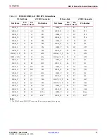
Страница 14: ...A1 H7 LA03_P 2 B1 G9 LA02_N 3 A2 H8 LA03_N 4 B2 G10 LA04_P 7 C1 H10 LA05_P 8 D1 D11 LA04_N 9 C2 H11 LA05_N 10 D2 D12 LA06_P 13 E1 C10 LA07_P 14 F1 H13 LA06_N 15 E2 C11 LA07_N 16 F2 H14 LA08_P 19 G1 G12 LA09_P 20 H1 D14 LA08_N 21 G2 G13 LA09_N 22 H2 D15 LA00_CC_P 25 I1 G6 LA01_CC_P 26 J1 D8 LA00_CC_N 27 I2 G7 LA01_CC_N 28 J2 D9 LA10_P 31 K1 C14 LA11_P 32 L1 H16 LA10_N 33 K2 C15 LA11_N 34 L2 H17 LA1...

Страница 15: ...LA20_N 4 B2 G22 LA21_P 7 C1 H25 LA22_P 8 D1 G24 LA21_N 9 C2 H26 LA22_N 10 D2 G25 LA23_P 13 E1 D23 LA24_P 14 F1 H28 LA23_N 15 E2 D24 LA24_N 16 F2 H29 LA25_P 19 G1 G27 LA26_P 20 H1 D26 LA25_N 21 G2 G28 LA26_N 22 H2 D27 LA17_CC_P 25 I1 D20 LA18_CC_P 26 J1 C22 LA17_CC_N 27 I2 D21 LA18_CC_N 28 J2 C23 LA27_P 31 K1 C26 LA28_P 32 L1 H31 LA27_N 33 K2 C27 LA28_N 34 L2 H32 LA29_P 37 M1 G30 LA30_P 38 N1 H34 L...

Страница 16: ...A07_N 16 F2 J10 HA08_P 19 G1 F10 HA09_P 20 H1 E9 HA08_N 21 G2 F11 HA09_N 22 H2 E10 HA00_CC_P 25 I1 F4 HA01_CC_P 26 J1 E2 HA00_CC_N 27 I2 F5 HA01_CC_N 28 J2 E3 HA10_P 31 K1 K13 HA11_P 32 L1 J12 HA10_N 33 K2 K14 HA11_N 34 L2 J13 HA12_P 37 M1 F13 HA13_P 38 N1 E12 HA12_N 39 M2 F14 HA13_N 40 N2 E13 HA14_P 41 O1 J15 HA15_P 42 P1 F16 HA14_N 43 O2 J16 HA15_N 44 P2 F17 HA16_P 47 Q1 E15 HA17_CC_P 48 R1 K16 ...

Страница 17: ...E25 HB07_N 16 F2 J28 HB08_P 19 G1 F28 HB09_P 20 H1 E27 HB08_N 21 G2 F29 HB09_N 22 H2 E28 HB00_CC_P 25 I1 K25 HB06_CC_P 26 J1 K28 HB00_CC_N 27 I2 K26 HB06_CC_N 28 J2 K29 HB10_P 31 K1 K31 HB11_P 32 L1 J30 HB10_N 33 K2 K32 HB11_N 34 L2 J31 HB12_P 37 M1 F31 HB13_P 38 N1 E30 HB12_N 39 M2 F32 HB13_N 40 N2 E31 HB14_P 41 O1 K34 HB15_P 42 P1 J33 HB14_N 43 O2 K35 HB15_N 44 P2 J34 HB16_P 47 Q1 F34 HB17_CC_P ...

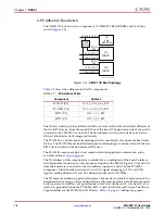
Страница 18: ...olled by a combination of the board interface and chip enable connections to the component inputs on the XM101 Signals GA0 and GA1 from the board are connected to the two address inputs A1 and A0 of the PCA9543 component Xilinx boards provide GA0 and GA1 signal strapping to 3 3V and GND signals creating different A0 and A1 address decodes on the PCA9543 The IIC memory addressing protocol requires ...

Страница 19: ...ster The two downstream IIC devices connected to the PCA9543 are at the same IIC address Si570 U1 IIC address is at 0x5D PCA9543 control register bits CR 1 0 01 Si570 U2 IIC address is at 0x5D PCA9543 control register bits CR 1 0 10 The U4 PCA9543 IIC bus switch to J1 FMC HPC connections are shown in Table 1 10 Table 1 8 PCA9543 IIC Switch Device Select Code Bit 7 4 Device Type Identifier Bit 3 Bi...

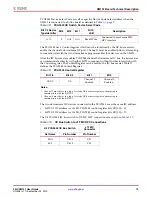
Страница 20: ... 1 11 For additional information on this component including reprogramming the clock frequency through the IIC serial bus interface consult the manufacturer s data sheet at www silabs com The U1 and U2 Si570 output clocks to J1 FMC HPC connections are shown in Table 1 12 Table 1 11 Characteristics of Si570 Component Si570 Characteristic XM101 Output Format LVDS Output Enable Polarity High Temperat...

Страница 21: ...ating different E0 and E1 chip enable decodes on the E1 and E0 inputs of the EEPROM The IIC memory addressing protocol requires a bus master to initiate communication to a peripheral device using a start condition followed by a device select code The device select code consists of a 4 bit Device Type Identifier and a 3 bit Chip Enable Address E2 E1 and E0 Bit 0 is used to indicate read write The D...

Страница 22: ...22 www xilinx com FMC XM101 User Guide UG538 v1 1 September 24 2010 Chapter 1 XM101 ...

Страница 23: ...Mouser Electronics Authorized Distributor Click to View Pricing Inventory Delivery Lifecycle Information Xilinx HW FMC XM101 G ...

Отзывы: