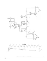
The signal shaper contains switching elements and a
diode array for signal conditioning the buffered
triangle and square inputs into the various waveforms
controlled by the function switch. The selected
waveform is the carrier (+ Y) input to the transcon-
ductance multiplier,
an integrated circuit, four-
quadrant multiplier.
The modulation (+X) input is a positive dc from the
control amplifier when the AM switch is off, providing
a fixed gain reference for the multiplier. Output cur-
rents from the multiplier are applied to the summing
node of the preamplifier for conversion to an inverted
voltage signal.
The preamplifier output is then attenuated by the front
panel amplitude control and fed to the output amplifier
summing node along with the dc offset control. The
output amplifier is an inverting amplifier whose output
is fed into step attenuator and then to the function
output connector.
The attenuator consists of a
distributed network having
output impedance.
This network provides attenuation in 20 dB (1/1 0)
steps to 60 dB.
For continuous operation of the basic function
generator loop (bold path in figure 4-1), the trigger
amplifier must maintain a positive level above the
most positive charge on the integrating capacitor in
order to reverse bias the start/stop diode. Thus, in
continuous mode the trigger logic senses the con-
tinuous control line from the front panel mode selec-
tor and holds the inverting trigger amplifier input low.
In triggered and gated modes the trigger amplifier out-
puts some level below the positive peak charging
level, and the start/stop diode is forward biased to
sink the current source and prevent the timing
capacitor from charging to the positive peak. This
stops waveform generation and holds the triangle out-
put at some dc level called the trigger baseline. The
trigger baseline is the level where a triangle, and thus
sine, waveform starts and stops when triggered or
gated.
The normal trigger baseline is zero volts, analogous to
0° phase of a sine or triangle waveform. The trigger
start/stop control offsets the trigger amplifier output
and can change the baseline for starting and stopping
a sine or triangle waveform from its negative peak
(- 90°) to its positive peak (+ 90°) At the extreme
positive peak level setting though, the diode is again
reverse biased and generator operation goes con-
tinuous, independent of generator mode.
While the integrating capacitor is being held from
charging, the start/stop diode must sink the current
source, which has a magnitude variable with VCG in-
puts. Therefore, a compensation is necessary to the
voltage level output by the trigger amplifier in order to
maintain a constant baseline level as VCG inputs, cur-
rent source magnitude and forward voltage drop by
the start/stop diode are varied. The baseline compen-
sation circuit measures the forward voltage across a
diode placed in the current source and injects an off-
setting current into the trigger amplifier to maintain an
equal voltage differential between the baseline level
and trigger amplifier output.
The trigger logic determines that after a waveform
starts, it always stops at a complete cycle and at the
same phase angle at which it started. The trigger logic
receives a trigger stimulus from the signal limiter and
latches the trigger amplifier output positive, allowing
the generator loop to run. When the negative peak of
the last cycle is reached (just one cycle in trigger
mode), the square from the hysteresis switch latches
the trigger amplifier back to its previous level. The in-
tegrating capacitor will charge back to the trigger
baseline where the start/stop diode once again for-
ward biases.
The generator mode switch sets the gated control line
to determine whether the trigger logic is to latch the
generator on for one cycle of for the duration of the
trigger stimulus.
The modulation generator board contains the power
supplies, the modulation generator and various
switching elements to control the source and type of
modulation and triggering signals to the main
generator.
The modulation generator is an integrated circuit
source of sine, triangle and square waveforms, whose
frequency is controllable by front panel multiplier
switch, variable control, and external voltage at the
FM IN input. The triangle and square are applied to a
ramp generator consisting of a balanced modulator
and buffer amplifier to produce ramp waveforms. A
modulation waveform or a SWP SET dc level is sent to
the function buffer via the front panel function selec-
tor.
The function buffer output is sent to the modulation
output
connector, the generator mode switch
for an internal trigger and gate stimulus, and the
amplitude buffer after being attenuated by the front
panel amplitude control. The amplitude buffer output
goes to the AM, FM and PM switches “internal” posi-
tions. The EXT MOD IN connector provides a connec-
4-2


