WM_PRJ_Q2400_PTS_005 -007
18th January 2006
Confidential©
All rights reserved
Page:
11
/
51
This document is the sole and exclusive property of WAVECOM. Not to be
distributed or divulged without prior written agreement.
2 Baseband Design
Note:
Some of the WISMO interface signals are multiplexed in order to limit number of
pins but this architecture implies some limitation.
For example in case of using SPI bus, 2-wire bus can not be used.
Warning:
All external signals must be inactive when the WISMO module is OFF to avoid
any damage when starting and allow WISMO module to start correctly.
2.1 Power supply and ground design rules
2.1.1 Electrical constraints
The power supply is one of the key issues in the design of a GSM terminal. Due
to the bursted emission in GSM / GPRS, the power supply must be able to
deliver high current peaks in a short time and assured that the voltage delivered
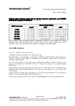
to the module remains always under the limits specified in the table “Maximum
voltage ripple (Uripp) vs Frequency in GSM & DCS” hereafter, specially during
burst while there is a drop of voltage (see Figure 1).
In communication mode, a GSM/GPRS class 2 terminal emits 577 µs radio bursts
every 4.615 ms.
In communication mode, a GPRS class 10 terminal emits 1154 µs radio bursts
every 4.615 ms.
Uripp
Uripp
T = 4.615 ms
t = 577 µs
VBATT
(1)
IBATT
(1)
or VDD if connected to VBATT
Vmax
Vmin
Figure 1: Typical power supply voltage in GSM mode
Two different inputs are provided for the power supply:
•
the first one, VBATT is used to supply the RF part,
•
the second one, VDD is used to supply the baseband part.
The power supply voltage features given in the table hereafter will guarantee
nominal functioning of the module.


