background image


10 

© 2020 Virginia Diodes, Inc.

—All Rights Reserved—Rev: 12 June 2020 


Responsivity vs. RF Input Power


The plot below is an example of how the responsivity changes as a function of RF input power for a specific WR10 detector at ~93 
GHz. For small signal RF input power, the detector is in the square law region, where the detector output voltage is proportional to 
the RF input power.  

The general shape of the curve is consistent for all diode detectors. However, the scale will vary with frequency and the detector 
design and other operating conditions, for example temperature.  

Responsivity vs. RF input power data can be supplied for all shipped ZBDs at an additional cost.  


Figure 1: Responsivity vs. RF Input Power 

The performance (responsivity vs. RF input power) is shown for a specific WR10ZBD at ~93 GHz.   


0

500

1000

1500

2000

2500

3000

-45

-40

-35

-30

-25

-20

-15

-10

-5

Respo

n

siv

it

y

 (

V

/W

)

RF Input Power (dBm)

Responsivity vs. RF Input Power

Responsivity vs. RF Input Power


Appendix 

Two


Содержание QOD

Страница 1: ...nd Street SE Suite 309 Charlottesville VA 22902 6172 USA Tel 434 297 3257 Fax 434 297 3258 www vadiodes com 2020 Virginia Diodes Inc All Rights Reserved Zero Bias Detector Operational Manual ZBD ZBD F QOD 2020 ...

Страница 2: ...e 4 5 Configurations ZBD vs ZBD F Page 6 Product Specifications Page 7 Appendix 1 ZBD Responsivity Performance Pages 8 9 ZBD Performance WR10 and WR6 5 Page 8 ZBD Performance WR5 1 and WR2 2 Page 9 Appendix 2 Responsivity vs RF Input Power Pages 10 Responsivity vs RF Input Power Page 10 Appendix 3 IF Amplifier Pre testing before use with VDI Detector Pages 11 Amplifier Pre testing before use with ...

Страница 3: ...using this device Virginia Diodes Inc VDI accepts no liability for damage or injury resulting from or caused by Improper use disassembly or use for purposes other than those for which the product was designed Use outside common safety health or general advisories pertaining to microwave millimeter wave and VDI products Repairs carried out by persons other than VDI or its assigned agents Waveguide ...

Страница 4: ...ons are for typical WR 3 4 zero bias detectors Other ZBDs WR 8 0 to WR 1 0 have similar configuration and dimensions High Frequency Zero Bias Detectors WR 0 8 to WR 0 65 The WR0 8ZBD has an integrated horn antenna 25dBi RF input port and a coaxial output The WR0 65ZBD has a rectangular waveguide RF input port and a coaxial output The drawing and corresponding dimensions are for a typical WR 0 65 a...

Страница 5: ...etector output port using a floating voltmeter See Page 6 for configuration details ZBD F Configuration using Bias Tee and Amplifier Appropriate voltages must be applied to the voltage pins on the provided amplifier ZBD F Configuration using External ESD Protection Circuit Monitor detector output port using a floating voltmeter See Page 6 for configuration details Black Backing Plate Unused ports ...

Страница 6: ...the ZBD compared to the other amplifier Therefore there will be less signal degradation through the amplifier included in the FDA option compared to the other amplifiers Amplifier gain performance assumes correct testing conditions bias voltage input impedance output impedance specified in the above table Fast Detector Options Fast Detector Option Frequency Range Gain dB typical Bias Voltage Input...

Страница 7: ...h Bias Tee and Amplifier 2 9mm f ZBD F with External ESD Protection 2 9mm f RF Input Power Linear typ 25 dBm 1dB Compression typ 20 dBm Maximum RF Input Power for ZBDs only Recommended Damage for WR15 to WR2 8 0 dBm 5 dBm Recommended Damage for all other ZBDs 3 dBm 0 dBm Maximum RF Input Power for ZBD Fs only Recommended Damage for WR0 65 only 3 dBm 0 dBm Recommended Damage for all other ZBD Fs 0 ...

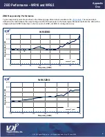
Страница 8: ...n the output voltage and the RF input power in the linear region Measured performance data will be shipped with each ZBD Data shown in this manual is for ZBD not ZBD F configurations only ZBD Performance WR10 and WR6 5 Appendix One 0 1000 2000 3000 4000 5000 6000 75 80 85 90 95 100 105 110 Responsivity V W Frequency GHz WR10ZBD Typical 0 1000 2000 3000 4000 5000 6000 110 120 130 140 150 160 170 Re...

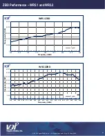
Страница 9: ... 1 and WR2 2 0 1000 2000 3000 4000 5000 140 150 160 170 180 190 200 210 220 Responsivity V W Frequency GHz WR5 1ZBD Typical 0 500 1000 1500 2000 2500 3000 3500 4000 330 340 350 360 370 380 390 400 410 420 430 440 450 460 470 480 490 500 Responsivity V W Frequency GHz WR2 2ZBD Typical ...

Страница 10: ...general shape of the curve is consistent for all diode detectors However the scale will vary with frequency and the detector design and other operating conditions for example temperature Responsivity vs RF input power data can be supplied for all shipped ZBDs at an additional cost Figure 1 Responsivity vs RF Input Power The performance responsivity vs RF input power is shown for a specific WR10ZBD...

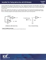
Страница 11: ...mplifier bias is applied rapidly Before using an amplifier with a VDI detector it is recommended that bias or turn on transients at the amplifier input be tested Attach a 1kΩ resistor to the input of the amplifier Monitor the resistor voltage on an oscilloscope as the amplifier bias is applied The turn on transient voltages across the resistor should be kept less than 100mV for safe operation Appe...

Страница 12: ...to continually improve our products We also depend upon feedback from colleagues and customers Ideas to simplify component operations improve performance or add capabilities are always welcome Contact VDI Virginia Diodes Inc Web http www vadiodes com Email Technical vadiodes com Telephone 434 297 3257 Addendum Product Updates and Company Contacts ...

Отзывы: