background image

11

Alignment

Introduction

The 

VX-2500V

 is carefully aligned at the factory for the

specified performance across the frequency range speci-
fied for each version. Realignment should therefore not
be necessary except in the event of a component failure,
or altering version type. All component replacement and
service should be performed only by an authorized Ver-
tex Standard representative,or the warranty policy may
be void.

The following procedures cover the sometimes critical and
tedious adjustments that are not normally required once
the transceiver has left the factory. However, if damage
occurs and some parts subsequently are placed, realign-
ment may be required. If a sudden problem occurs dur-
ing normal operation, it is likely due to component fail-
ure; realignment should not be done until after the faulty
component has been replaced.

We recommend that servicing be performed only by au-
thorized Vertex Standard service technicians who are ex-
perienced with the circuitry and fully equipped for repair
and alignment. Therefore, if a fault is suspected, contact
the dealer from whom the transceiver was purchased for
instructions regarding repair. Authorized Vertex Standard
service technicians realign all circuits and make complete
performance checks to ensure compliance with factory
specifications after replacing any faulty components.

Those who do undertake any of the following alignments
are cautioned to proceed at their own risk. Problems
caused by unauthorized attempts at realignment are not
covered by the warranty policy. Also, Vertex Standard
reserves the right to change circuits and alignment proce-
dures in the interest of improved performance, without
notifying owners.

Under no circumstances should any alignment be attempt-
ed unless the normal function and operation of the trans-
ceiver are clearly understood, the cause of the malfunc-
tion has been clearly pinpointed and any faulty compo-
nents replaced, and realignment determined to be abso-
lutely necessary.

The following test equipment (and thorough familiarity
with its correct use) is necessary for complete realignment.
Correction of problems caused by misalignment result-
ing from use of improper test equipment is not covered
under the warranty policy. While most steps do not re-
quire all of the equipment listed, the interactions of some
adjustments may require that more complex adjustments
be performed afterwards.

Do not attempt to perform only a single step unless it is
clearly isolated electrically from all other steps. Have all
test equipment ready before beginning, and follow all of
the steps in a section in the order presented.

Required Test Equipment

r

RF Signal Generator with calibrated output level
at 500MHz

r

Deviation Meter (linear detector)

r

In-line Wattmeter with 5% accuracy at 1000MHz

r

50

W

 RF Dummy Load with power rating 100W

at 500MHz

r

4

W

 AF Dummy Load

r

Regulated DC Power Supply (standard 13.8V
DC, 15A)

r

Frequency Counter with 0.1ppm accuracy at
500MHz

r

AC Voltmeter

r

DC Voltmeter

r

VHF Sampling Coupler

r

IBM PC/compatible Computer

r

Oscilloscope

r

Vertex Standard 

VPL-1

 Connection Cable &

Alignment program

Alignment Preparation & Precautions

A 50

W

 RF Dummy Load and in-line wattmeter must be

connected to the main antenna jack in all procedures that
call for transmission, except where specified otherwise.
Correct alignment is not possible with an antenna.

After completing one step, read the following step to de-
termine whether the same test equipment will be required.
If not, remove the test equipment (except dummy load
and wattmeter, in connected) before proceeding.

Correct alignment requires that the ambient temperature
be the same as that of the transceiver and test equipment,
and that this temperature be held constant between 68°F
and 86°F (20°C ~ 30°C). When the transceiver is brought
into the shop from hot or cold air, it should be allowed
time to come to room temperature before alignment.

Whenever possible, alignments should be made with os-
cillator shields and circuit boards firmly affixed in place.

Also, the test equipment must be thoroughly warmed up
before beginning.

Note: 

Signal levels in dB referred to in the alignment pro-

cedure are based on 

0dB

m

 EMF = 0.5

m

V.

Содержание VX-2500V

Страница 1: ...n in this manual to be correct Vertex Standard assumes no liability for damage that may occur as a result of typographical or other errors that may be present Your cooperation in pointing out any inconsistencies in the technical information would be appreciated Specifications 2 DSUB 9 pin Accessory Connector 3 Exploded View Miscellaneous Parts 4 Block Diagram 5 Interconnection Diagram 7 Circuit De...

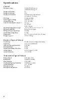
Страница 2: ... Impedance 50 ohms Audio Output Impedance 4 ohms Dimensions 6 3 x 1 6 x 4 3 inch 160 x 40 x 110 mm Weight Approx 1 87 lb 0 85 kg Receiver Typical Values Circuit type Double conversion Super heterodyne Sensitivity 0 25 uV 12 dB SINAD Adjacent Channel Selectivity 80 70 dB Intermodulation 75 dB Spurious and Image Rejection 90 dB Audio Output 4 W 4 ohms 5 THD Audio Distortion 3 1 kHz Transmitter Typic...

Страница 3: ...switch the radio operation between dispatch operation and Data mode DTR Low Turn on the Data transmission less than 0 5 V DTR High Turn off the Data transmission more than 4 0 V Pin 5 Ground Pin 6 Output Horn alert signal Open collector with maximum 16 0 V 100 mA sink Pin 7 Input external PTT Low Request the transmission High Request the Receiving Pin 8 Output supply voltage Need to set the solder...

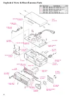
Страница 4: ... RA0060700 PM HOLDER RA0066400 FERRITE BEADS L9190001 WIRE ASSY T9206633 SPEAKER M4090154 BLIND SEET 4 x 3 RA0405200 WIRE ASSY T9206979 PANEL UNIT MAIN UNIT CONNECTOR P1090984 CONNECTOR P1090654 WIRE ASSY T9206634A IC G1093557 REF ƒ QTY 1 2 2 4 1 7 DESCRIPTION BINDING HEAD SCREW M2 6 x 6 NI BINDING HEAD SCREW M3 x 6 NI BINDING HEAD SCREW M3 x 8 NI TAPTITE SCREW M3 x 6 NI TAPTITE SCREW M3 x 8 OVAL ...

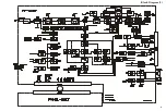
Страница 5: ...5 Block Diagram 1 ...

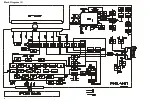
Страница 6: ...6 Block Diagram 2 ...

Страница 7: ...7 Interconnection Diagram ...

Страница 8: ...8 Note ...

Страница 9: ...y the FM detector CD1001 CDBC450CX24 Detected audio from Q1029 is applied to Q2016 AK2345 and audio low pass filter After volume adjustment by Q2014 M62364FP the audio signal is amplified by the AF power amplifier Q1509 TDA2003H and passed to speaker jack 4 Transmit Signal Path Voice audio from the microphone is delivered via the MIC Jack Unit to the PANEL Unit after passing through amplifier Q202...

Страница 10: ...Q2016 AK2345 6 3 MPU Operation is controlled by 8 bit MPU IC Q2013 LC87F72C8A The system clock uses a 3 6864MHz crys tal for a time base IC Q2003 S 80735SN resets the MPU when the power is on and monitors the voltage of the regulated 5V power supply line 6 4 DCS LTR Encorder The DCS code is generation and encoding by MPU IC Q2013 LC87F72C8A It is filtered by Q2021 NJM2902V and adjusted the level b...

Страница 11: ...ollowing test equipment and thorough familiarity with its correct use is necessary for complete realignment Correction of problems caused by misalignment result ing from use of improper test equipment is not covered under the warranty policy While most steps do not re quire all of the equipment listed the interactions of some adjustments may require that more complex adjustments be performed after...

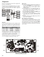
Страница 12: ...quency With the wattmeter dummy load and frequency counter connected to the antenna jack and select band center fre quency channel key the transmitter and adjust VR1001 on the RF Unit if necessary so the counter frequency is within 100 Hz of the channel center frequency for the trans ceiver version Alignment Important In order to facilitate alignment over the complete switch ing range of the equip...

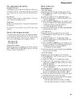
Страница 13: ...P or DWN key as needed to set the power output to the following specification as indicated on the external wattmeter Tx Power High 25 W 0 5W When the 25 Watt level is attained press Enter to lock in the new data 1 Tx Power Low This parameter is used to align TX Low power 5W Press Enter on 1 Tx Power Low to align TX Low power Select the Channel 1 in alignment range Press the Space key on the keyboa...

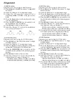
Страница 14: ...l DCS Deviation Wide 0 70 kHz Actual DCS Deviation Narrow 0 35 kHz 6 LTR Deviation This parameter is used to align the LTR deviation Press Enter on 6 LTR Deviation to align LTR Deviation Select the Channel 1 in alignment range Press the Space key on the keyboard to acti vate the transmitter and injects a LTR test tone Press the UP or DWN key as needed to set the LTR Deviation Wide to the following...

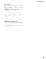
Страница 15: ...ge 1 Threshold NSQL This parameter is used to align the noise level in squelch Threshold It adjusts this alignment RX Tuning after end ing Select the MID frequency channel in alignment range Set the SG output level to 7dBm EMF and obey the message 2 RX Tune This parameter is used to align RX Tune Select the MID frequency channel in alignment range Set the SG output level to 6dBm EMF Pressing the D...

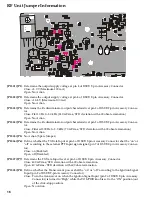
Страница 16: ...ith 600 ohm termination Open No Action JP1505 JP5 No Action Spare Jumper JP1506 JP6 Define whether the TX Data Input at pin 3 of DSUB 9 pin Accessory Connector shall be on or off according to the external PTT Input signal signal pin 7 of DSUB 9 pin Accessory Connec tor Close on Enabled Open off Disabled JP1507 JP7 Determine the TX Data Input level at pin 3 of DSUB 9 pin Accessory Connector Close 4...

Страница 17: ... RX 4 6 V TX 0 V RX 3 8 V TX 0 V RX 2 3 V TX 0 V RX 0 4 V TX 0 V RX 8 7 V TX 0 V 0 V 0 7 V 8 4 V 2 5 V 5 0 V 0 V 3 0 V 1 7 V 3 8 V 4 9 V RX 0 V TX 1 9 V RX 0 V TX 8 1 V RX 0 V TX 4 2 V RX 0 V TX 3 0 V RX 0 V TX 2 6 V RX 4 3 V TX 0 V 8 0 V 0 4 V 0 7 V 4 7 V WIDE 0 4 V NARROW 2 2 V WIDE 2 3 V NARROW 0 V WIDE 1 8 V NARROW 1 6 V WIDE 1 8 V NARROW 1 6 V WIDE 0 4 V NARROW 2 2 V 1 0 V 4 7 V 4 6 V 4 1 V 1...

Страница 18: ...OFF 8 9 V HORN ACTIVE 0 V HORN OFF 8 9 V HORN ACTIVE 8 3 V HORN OFF 0 V HORN ACTIVE 5 0 V BUSY 4 2 V MUTE 0 V BUSY 5 0 V MUTE 0 V BUSY 0 V MUTE 13 7 V 0 8 V 0 9 V 1 3 V 0 8 V 0 V 1 6 V 13 8 V 13 1 V 7 3 V RX 0 3 V TX 0 V 3 7 V 3 7 V 8 5 V 3 7 V 3 7 V 1 2 V 0 7 V 3 7 V 3 7 V RX WIDE 0 2 3 8 V RX NARROW 0 2 3 5 V TX 0 2 V RX WIDE 0 8 3 8 V RX NARROW 0 8 3 1 V TX 0 8 V RX WIDE 0 3 5 6 V RX NARROW 0 3...

Страница 19: ...68CB CB Q1504 2SK508 K52 Q1013 3SK228 XR Q1026 IMH6A H6 Q1017 M5223 Q1019 NJM2902V Q1003 1503 RT1N241M N2 Q1002 1006 1016 1032 1033 1034 1035 1502 1506 1507 1512 1518 SA7025DK Q1023 TDA2003H Q1509 2SC4154 LE Q1501 2SC4226 R22 Q1011 1015 2SC5107 MF0 Q1518 HSM88AS C1 D1011 1012 MC2850 A7 D1506 1507 ...

Страница 20: ...9 2SB1201S Q1005 2SC4116 LG Q1001 2SC4154 LE Q1007 1519 2SC4215Y QY Q1029 2SC5107 MFO Q1020 1021 1025 2SC5415E EA Q1022 2SJ125D JD Q1515 DTB123EK F12 Q1008 IMH6A H6 Q1010 MM1216ENRE Q1004 NJM78L05 Q1024 PDTC114TE 24 Q1508 1510 RT1N241M N2 Q1012 1030 1516 1517 MC2850 A7 D1501 1502 1503 1SS321 F9 D1022 MC2848 A6 D1024 1026 ...

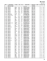
Страница 21: ...74227 1 A C3 C 1038 CHIP CAP 470pF 50V CH GRM39CH471J50PT K22174249 1 B c3 C 1039 CHIP CAP 0 001uF 50V B GRM39B102K50PT K22174821 1 A D1 C 1040 CHIP CAP 7pF 50V CH GRM39CH070D50PT K22174208 1 A G1 C 1041 CHIP CAP 2pF 50V CK GRM39CK020C50PT K22174203 1 B b3 C 1042 CHIP CAP 18pF 50V CH GRM39CH180J50PT K22174217 1 A G1 C 1043 CHIP CAP 0 001uF 50V B GRM39B102K50PT K22174821 1 A D1 C 1044 CHIP CAP 12pF...

Страница 22: ...RM39B102K50PT K22174821 1 B e2 C 1126 FILM CAP 0 022uF 16V ECHU1C223JB5 K57120011 1 B e3 C 1127 CHIP TA CAP 4 7uF 10V TEMSVA1A475M 8R K78100022 1 B d3 C 1128 CHIP CAP 22pF 50V CH GRM39CH220J50PT K22174219 1 A D3 C 1129 CHIP CAP 15pF 50V CH GRM39CH150J50PT K22174215 1 A D3 C 1130 CHIP CAP 47pF 50V CH GRM39CH470J50PT K22174227 1 A G3 C 1131 CHIP CAP 220pF 50V CH GRM39CH221J50PT K22174243 1 B d3 C 11...

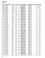
Страница 23: ...0J50PT K22174223 1 B e3 C 1204 CHIP CAP 0 001uF 50V B GRM39B102K50PT K22174821 1 A G3 C 1205 CHIP CAP 0 001uF 50V B GRM39B102K50PT K22174821 1 A C3 C 1206 CHIP CAP 0 01uF 50V B GRM39B103M50PT K22174823 1 B d2 C 1207 CHIP CAP 2pF 50V CK GRM39CK020C50PT K22174203 1 B b3 C 1208 CHIP CAP 0 001uF 50V B GRM39B102K50PT K22174821 1 B d2 C 1209 CHIP CAP 0 001uF 50V B GRM39B102K50PT K22174821 1 A C3 C 1210 ...

Страница 24: ...39CH150J50PT K22174215 1 A G1 C 1298 CHIP CAP 220pF 50V CH GRM39CH221J50PT K22174243 1 A G2 C 1299 CHIP CAP 15pF 50V CH GRM39CH150J50PT K22174215 1 C 1501 CHIP CAP 100pF 50V CH GRM39CH101J50PT K22174235 1 A B1 C 1502 CHIP CAP 100pF 50V CH GRM39CH101J50PT K22174235 1 B g1 C 1503 CHIP CAP 100pF 50V CH GRM39CH101J50PT K22174235 1 A A1 C 1504 CHIP CAP 100pF 50V CH GRM39CH101J50PT K22174235 1 B g1 C 15...

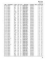
Страница 25: ...0704 1 B g3 D 1502 DIODE MC2850 T11 1 G2070704 1 B g3 D 1503 DIODE MC2850 T11 1 G2070704 1 B g1 D 1504 DIODE BAS316 G2070716 1 B g2 D 1505 DIODE D1F20 4063 G2070474 1 B f1 D 1506 DIODE MC2850 T11 1 G2070704 1 A B3 D 1507 DIODE MC2850 T11 1 G2070704 1 A B3 F 1501 CHIP FUSE 0 25A KAB 2402 251NA31 Q0000085 1 A B1 J 1501 CONNECTOR IL FPR 36S VF E1500 P1091126 1 A B3 J 1502 CONNECTOR AE0031 00 P1090998...

Страница 26: ...87 1 A G3 Q 1028 IC TA31136FN EL G1091605 1 B c3 Q 1029 TRANSISTOR 2SC4215Y TE85R G3342157Y 1 B c3 Q 1030 TRANSISTOR RT1N241M T11 1 G3070249 1 B b4 Q 1031 TRANSISTOR 2SA1602A T11 1F G3116028F 1 B c3 Q 1032 TRANSISTOR RT1N241M T11 1 G3070249 1 A E1 Q 1033 TRANSISTOR RT1N241M T11 1 G3070249 1 A D1 Q 1034 TRANSISTOR RT1N241M T11 1 G3070249 1 A E1 Q 1035 TRANSISTOR RT1N241M T11 1 G3070249 1 A E1 Q 150...

Страница 27: ... 16W 5 RMC1 16 474JATP J24185474 1 B e3 R 1051 CHIP RES 470k 1 16W 5 RMC1 16 474JATP J24185474 1 B d3 R 1052 CHIP RES 10k 1 16W 5 RMC1 16 103JATP J24185103 1 B e4 R 1053 CHIP RES 4 7k 1 16W 5 RMC1 16 472JATP J24185472 1 B e3 R 1054 CHIP RES 100k 1 16W 5 RMC1 16 104JATP J24185104 1 A G3 R 1055 CHIP RES 120 1 10W 5 RMC1 10T 121J J24205121 1 B e2 R 1056 CHIP RES 2 7 1 10W 5 RMC1 10T 2R7J J24205279 1 ...

Страница 28: ...23JATP J24185223 1 B c3 R 1131 CHIP RES 12k 1 16W 5 RMC1 16 123JATP J24185123 1 B b3 R 1132 CHIP RES 12k 1 16W 5 RMC1 16 123JATP J24185123 1 B b3 R 1134 CHIP RES 220k 1 16W 5 RMC1 16 224JATP J24185224 1 B c3 R 1135 CHIP RES 0 1 16W 5 RMC1 16 000JATP J24185000 1 A E1 R 1136 CHIP RES 22k 1 16W 5 RMC1 16 223JATP J24185223 1 B c3 R 1137 CHIP RES 2 2k 1 16W 5 RMC1 16 222JATP J24185222 1 B b3 R 1138 CHI...

Страница 29: ...6W 5 RMC1 16 472JATP J24185472 1 A A1 R 1539 CHIP RES 150k 1 16W 5 RMC1 16 154JATP J24185154 1 A B3 R 1540 CHIP RES 4 7k 1 16W 5 RMC1 16 472JATP J24185472 1 A B1 R 1541 CHIP RES 180 1 16W 5 RMC1 16 181JATP J24185181 1 A B3 R 1542 CHIP RES 2 2k 1 16W 5 RMC1 16 222JATP J24185222 1 A B3 R 1543 CHIP RES 680 1 16W 5 RMC1 16 681JATP J24185681 1 B g1 R 1544 CHIP RES 220k 1 16W 5 RMC1 16 224JATP J24185224...

Страница 30: ...30 REF DESCRIPTION VALUE V W TOL MFR S DESIG VXSTD P N VERS LOT SIDE LAY ADR RF Unit Parts List Note ...

Страница 31: ...TE 5 2 V FLASH ROM WRITE 12 0 V PTT ON 5 0 V PTT OFF 0 V 1 6 V 3 2 V 4 9 V 1 8 V 1 8 V 1 3 V 2 3 V 1 3 V 1 0 V 5 0 V 0 6 V 2 6 V 0 5 V 2 6 V 1 8 V 1 8 V 1 8 V 1 8 V 0 8 V 5 0 V 0 8 V 5 0 V 0 8 V 0 8 V 4 9 V 0 8 V 3 0 V 2 7 V 2 5 V 2 5 V 2 5 V 2 5 V 2 4 V 2 5 V 2 5 V 1 8 V 1 8 V 2 5 V 2 5 V 1 8 V 1 8 V 1 8 V 2 5 V 2 5 V 2 5 V 2 9 V 2 5 V 4 9 V 5 0 V COMPANDER OFF 0 V COMPANDER ON 5 0 V 2 5 V 2 5 V ...

Страница 32: ...PANEL Unit 32 Note ...

Страница 33: ...PANEL Unit 33 Parts Layout Side A A C B E D G F H 1 2 LC87F72C8A Q2013 BU4066BF Q2024 S 93C56AMFN Q2011 2SC4617 BR Q2004 2020 BRPG1211C D2004 DA221 K D2003 2033 2034 MC2846 A4 D2011 S 80835CNMC Q2003 ...

Страница 34: ... b e d g f h 1 2 AK2345 Q2016 M62364FP Q2014 LA8630M Q2017 NJM2902V Q2015 2021 2022 NJM78L05 Q2006 2SC4617 BR Q2001 2002 2005 2007 PDTC144EE 08 Q2019 RT1N241M N2 Q2008 2010 2025 RT1P441U P3 Q2009 DA221 K D2001 2002 2005 2009 2012 2013 2036 ...

Страница 35: ...08806 1 B g2 C 2036 CHIP CAP 0 0047uF 25V B TMK105B472KW F K22148831 1 B f2 C 2037 CHIP CAP 22pF 50V CH UMK105CH220JW F K22178266 1 B g2 C 2038 CHIP CAP 0 1uF 10V BJ LMK105BJ104KV F K22108806 1 B g2 C 2040 CHIP CAP 1uF 10V F GRM39F105Z10PT K22105001 1 B c1 C 2041 CHIP CAP 10pF 50V CH UMK105CH100DW F K22178258 1 B d1 C 2042 CHIP CAP 0 0018uF 50V B UMK105B182KW F K22178832 1 A D1 C 2043 CHIP CAP 560...

Страница 36: ...ODE MA2S111 TX G2070614 1 A B1 D 2008 LED TLOU262 G2090763 1 A B1 D 2009 DIODE DA221 TL G2070178 1 B c2 D 2010 DIODE MA2S111 TX G2070614 1 A B1 D 2011 DIODE MC2846 T11 1 G2070702 1 A A1 D 2012 DIODE DA221 TL G2070178 1 B h2 D 2013 DIODE DA221 TL G2070178 1 B d2 D 2014 DIODE MA2S111 TX G2070614 1 B e1 D 2015 DIODE MA2S111 TX G2070614 1 A D2 D 2016 DIODE MA2S111 TX G2070614 1 A C2 D 2017 DIODE MA2S1...

Страница 37: ...C1 16S 102JTH J24189025 1 B e2 R 2032 CHIP RES 10k 1 16W 5 RMC1 16S 103JTH J24189037 1 A C2 R 2033 CHIP RES 10k 1 16W 5 RMC1 16S 103JTH J24189037 1 B f1 R 2034 CHIP RES 2 2k 1 16W 5 RMC1 16S 222JTH J24189029 1 B h2 R 2035 CHIP RES 0 1 16W 5 RMC1 16S JPTH J24189070 1 B f2 R 2036 CHIP RES 220k 1 16W 5 RMC1 16S 224JTH J24189053 1 B f2 R 2037 CHIP RES 47k 1 16W 5 RMC1 16S 473JTH J24189045 1 A C1 R 203...

Страница 38: ... RMC1 16S 564JTH J24189058 1 B c2 R 2108 CHIP RES 47k 1 16W 5 RMC1 16S 473JTH J24189045 1 A D2 R 2109 CHIP RES 47k 1 16W 5 RMC1 16S 473JTH J24189045 1 B d1 R 2110 CHIP RES 1 2M 1 16W 5 RMC1 16S 125JTH J24189062 1 B d2 R 2111 CHIP RES 150k 1 16W 5 RMC1 16S 154JTH J24189051 1 B c2 R 2112 CHIP RES 47k 1 16W 5 RMC1 16S 473JTH J24189045 1 B e2 R 2113 CHIP RES 220k 1 16W 5 RMC1 16S 224JTH J24189053 1 B ...

Страница 39: ...H J24189070 1 B d1 R 2181 CHIP RES 1M 1 16W 5 RMC1 16S 105JTH J24189061 1 B e2 S 2001 TACT SWITCH SKQMAQE010 N5090121 1 A B2 S 2002 TACT SWITCH SKQMAQE010 N5090121 1 A C2 S 2003 TACT SWITCH SKQMAQE010 N5090121 1 A D2 S 2004 TACT SWITCH SKQMAQE010 N5090121 1 A E1 S 2005 TACT SWITCH SKQMAQE010 N5090121 1 A E1 S 2006 TACT SWITCH SKQMAQE010 N5090121 1 A E2 S 2007 TACT SWITCH SKQMAQE010 N5090121 1 A F2...

Страница 40: ...40 REF DESCRIPTION VALUE V W TOL MFR S DESIG VXSTD P N VERS LOT SIDE LAY ADR PANEL Unit Parts List Note ...

Страница 41: ...18 Copyright 2003 VERTEX STANDARD CO LTD All rights reserved No portion of this manual may be reproduced without the permission of VERTEX STANDARD CO LTD ...

Отзывы: