background image


ODIN-W2 series - System integration manual 

UBX-14040040 - R20 

Handling and soldering


Page 32 of 43 

C1-Public 


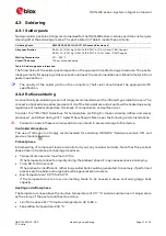
Cooling phase 

A controlled cooling avoids negative metallurgical effects (solder becomes more brittle) of the solder 
and possible mechanical tension in the products. Controlled cooling helps to achieve bright solder 
fillets with a good shape and low contact angle. 


Temperature fall rate: max 2 °C/s between 200 °C and a higher peak temperature; max 4 °C/s when 
the temperature is below 200 °C. 


The modules should be placed on the topside of the motherboard during soldering to avoid falling 
off.  

The soldering temperature profile chosen at the factory depends on additional external factors like 
choice of soldering paste, size, thickness and properties of the base board and so on.  


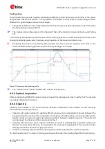
Exceeding the maximum soldering temperature and the maximum liquidus time limit in the 
recommended soldering profile can permanently damage the module. 


Figure 11: Recommended soldering profile 


The modules must not be soldered with a damp heat process.  

4.3.3


Optical inspection 

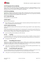
After soldering the ODIN-W2 series modules, inspect the modules optically to verify that the module 
is properly aligned and centered. 

4.3.4


Cleaning 

Cleaning the modules is not recommended. Residues underneath the modules cannot be easily 
removed with a washing process. 


Cleaning with water will lead to capillary effects where water is absorbed in the gap between the 
baseboard and the module. The combination of residues of soldering flux and encapsulated water 
leads to short circuits or resistor-like interconnections between neighboring pads. The water will 
also damage the sticker and the ink-jet printed text. 


Cleaning with alcohol or other organic solvents can result in soldering flux residues flooding into 
the two housing areas that are not accessible for post-wash inspections. The solvent will also 
damage the sticker and the ink-jet printed text. 


Ultrasonic cleaning will permanently damage the module especially, the quartz oscillators. 

For best results use a “no clean” soldering paste and eliminate the cleaning step after the soldering. 

Содержание ODIN-W2 Series

Страница 1: ...em integration manual Abstract This document describes the system integration of ODIN W2 series multiradio modules The ODIN W2 module is a compact stand alone dual band Wi Fi Bluetooth dual mode Bluet...

Страница 2: ...data will be published later Objective Specification Target values Revised and supplementary data will be published later Advance Information Data based on early testing Revised and supplementary dat...

Страница 3: ...1 4 1 Module reset 14 1 4 2 External low power clock for power saving modes 14 1 4 3 System input and output signals 14 1 4 4 Restoring default configuration 15 1 5 Data communication interfaces 15 1...

Страница 4: ...PO_CLK design 25 3 6 General High Speed layout guidelines 25 3 6 1 General considerations for schematic design and PCB floor planning 26 3 6 2 Module placement 26 3 6 3 Layout and manufacturing 26 3 7...

Страница 5: ...34 6 Product testing 35 6 1 u blox In Series production test 35 6 2 OEM manufacturer production test 35 6 2 1 Go No go tests for integrated devices 36 Appendix 37 A Glossary 37 B Checklist 38 B 1 Sch...

Страница 6: ...rt includes dual mode Bluetooth v4 0 BR EDR and low energy and dual band Wi Fi 2 4 and 5 GHz bands The module supports point to point and point to multipoint configurations and can have concurrent Blu...

Страница 7: ...ODIN W2 series System integration manual UBX 14040040 R20 System description Page 7 of 43 C1 Public Table 1 Key features of ODIN W2 series ODIN W260 ODIN W262 ODIN W263...

Страница 8: ...antennas The MIMO port functionality is available only in the ODIN W260 module Different antenna options are available depending on the chosen ODIN W2 series model ODIN W260 A standard coaxial U FL co...

Страница 9: ...n needed and ensures that no transmissions occur simultaneously 1 1 5 u blox connectivity software The ODIN W2 module is pre flashed with u blox connectivity software See the u connectXpress software...

Страница 10: ...n description Figure 2 ODIN W2 series pin assignment The signals are available on castellation pads on the edge of the PCB The unfilled circular pads are GND pads Black circular pads are test and prod...

Страница 11: ...Green LED Signal System Input Signal Active low The GREEN signal is not valid until 500 ms after the startup RESET_N pin is released or power is applied If the level on this pin is pulled down during...

Страница 12: ...A15 8 D1 PD_8 IO UART3 not used for u blox connectivity software UART3 CTS A16 9 D6 PD_11 IO UART3 not used for u blox connectivity software UART3 RTS A17 10 D7 PD_12 IO UART3 not used for u blox conn...

Страница 13: ...3 Summary of voltage supply requirements The ODIN W2 series modules must be supplied with a proper DC power supply through the VCC pins which can be one of the following Switching Mode Power Supply S...

Страница 14: ...u blox Short Range AT Commands Manual 1 for more information about the different power saving modes The clock must be available during start up after power on or while leaving the reset state See the...

Страница 15: ...S should be connected to GND on the ODIN W2 module The use of flow control is configured with an AT command See the u blox Short range AT commands manual 1 for more information The Link status pins DT...

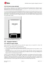
Страница 16: ...PHY side Follow the recommendations from the selected PHY chip for implementation details An example of a PHY implementation is shown in Figure 3 The PHY KSZ8081 is the recommended PHY that is used on...

Страница 17: ...is different for each module version in the ODIN W2 series 1 6 1 Antenna connectors The ODIN W260 module has two RF antenna U FL connectors with a characteristic impedance of 50 The main supports bot...

Страница 18: ...not connect reserved RSVD pin The reserved pins can be allocated for future interfaces and functionality 1 9 GND pins Good connection of the module s GND pins with solid ground layer of the host appli...

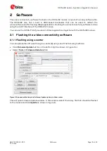
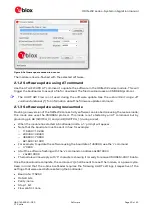
Страница 19: ...ace of the ODIN W2 module You can use the SWD JTAG if you use Arm Mbed applications together with the ODIN W2 module 2 1 Flashing the u blox connectivity software 2 1 1 Flashing using s center You can...

Страница 20: ...mode also uses the XMODEM protocol This mode is not started by an AT command but by grounding pin A6 SWITCH_0 and pin A8 SWITCH_1 during a reset When the module has started in bootloader mode a prompt...

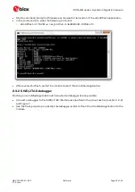
Страница 21: ...le Start a command prompt in Windows and browse to the location of the stm32flash application In the command line write the following command o stm32flash b 115200 w sw_bin file S 0x8000000 COMport Re...

Страница 22: ...32flash b 115200 w sw_bin file S 0x8000000 COMport After successful flash restart the module to start the Arm Mbed application 2 3 2 SWD JTAG debugger Flashing an Arm Mbed application with an external...

Страница 23: ...schematic and layout design 4 Other pins Accurate design is required to guarantee proper functionality Follow the recommendations provided in section 3 6 for schematic and layout design 3 2 Antenna in...

Страница 24: ...nterfaces 3 3 1 Module supply design Good connection of the module s VCC pin with DC supply source is required for correct RF performance The guidelines are summarized below VCC connection must be as...

Страница 25: ...bus should be done so that noise injection and cross talk are avoided See the Schematic for ODIN W2 section for additional information It is recommended to use the hardware flow control with RTS CTS t...

Страница 26: ...cement allows better RF performance See section 1 6 for more information on antenna consideration during module placement The heat dissipation during continuous transmission at maximum power can signi...

Страница 27: ...IN W2 series modules The proposed land pattern layout reflects the pads layout of the modules and extends 0 2 mm outside the module outline The Non Solder Mask Defined NSMD pad type is recommended ove...

Страница 28: ...the end product in such a way that it provides good thermal dissipation Force ventilation air flow within the mechanical enclosure Provide a heat sink component attached to the application board on t...

Страница 29: ...egration manual UBX 14040040 R20 Design in Page 29 of 43 C1 Public The RESET_N should be driven from a GPIO on the host platform to enable reset restore functionality Figure 10 A complete ODIN W2 desi...

Страница 30: ...ing area The main principle of an EPA is that there are no highly charging materials near ESD sensitive electronics all conductive materials are grounded workers are grounded and charge build up on ES...

Страница 31: ...ly regardless of material properties thickness of components and surface color Consider the IPC 7530 Guidelines for temperature profiling for mass soldering reflow and wave processes published during...

Страница 32: ...d soldering profile The modules must not be soldered with a damp heat process 4 3 3 Optical inspection After soldering the ODIN W2 series modules inspect the modules optically to verify that the modul...

Страница 33: ...of the modules and it is important to prevent them from flowing into the module The RF shields do not provide protection for the module from coating liquids with low viscosity therefore care is requi...

Страница 34: ...Page 34 of 43 C1 Public 5 Qualifications and approvals ODIN W263 is configured to always support the ETSI domain and is only allowed to be used in countries allowing ETSI domain channels See ODIN W2...

Страница 35: ...programming Measurement of current Functional tests Digital I O tests Measurement and verification of RF characteristics in all supported bands calibration not needed since performed automatically by...

Страница 36: ...with an external AP or station Example commands that can be used to get the signal quality are AT UBTI Bluetooth Inquiry AT UBTD BLE Discovery AT UWSCAN WiFi Scan More information about the AT comman...

Страница 37: ...and Electronics Engineers I2C Inter Integrated Circuit L Low LDO Low Drop Out LPO Low Power Oscillator MCU Microcontroller MIMO Multi Input Multi Output N A Not Applicable O Output means that this is...

Страница 38: ...ions if applied 7 Check UART signal direction 8 Provide proper precautions for ESD immunity as required on the application board Table 8 Schematic checklist B 2 Layout checklist No Description Status...

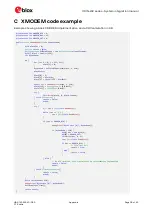
Страница 39: ...lock 3 128 blockCnt block 0 1 block 1 blockCnt block 2 byte 255 blockCnt ushort crc xmodemCalcrc block 3 128 block 131 Byte crc 8 0xFF block 132 Byte crc 0xFF try this Write block 0 block Length catch...

Страница 40: ...yte data buffer in the xmodem block count number of data bytes offset where to start the calculation private ushort xmodemCalcrc byte buffer int offset int count ushort crc i int j crc 0 for j offset...

Страница 41: ...BX 14039949 3 u connectXpress software user guide UBX 16024251 4 u blox Package information guide document number UBX 14001652 5 stm32flash exe http stm32flash sourceforge net 6 s center evaluation so...

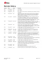
Страница 42: ...and Appendix C R08 03 Jan 2017 kgom Included support for ODIN W2 firmware versions 2 0 2 and 3 0 1 On page 2 replaced Document status with Disclosure restriction R09 30 Mar 2017 fbro kgom Included su...

Страница 43: ...com Regional Office China Beijing Phone 86 10 68 133 545 E mail info_cn u blox com Support support_cn u blox com Regional Office China Chongqing Phone 86 23 6815 1588 E mail info_cn u blox com Suppor...

Отзывы: