


EVK-IRIS-W10 - User guide
UBX-23007837 - R03
Hardware description
Page 23 of 43
C1-Public
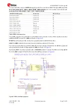
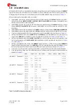
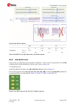
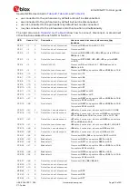
The IRIS-W10 module
SWD
interface,
GPIO13-SWDCLK
and
GPIO14-SWDIO
, are connected
to the MCU-LINK interface and
J45
needles connector simultaneously by default through
0R
resistors
R2 and R12
those
GPIOs
could be also connected to
J20
by disconnecting the last
two resistors and populate
resistors
R48, R116
with
0 R.
See connections in
GPIOs
13
and
14
are also accessible through pin headers
J47 (
pin 2) and
J48 (
pin 1)
,
respectively. By toggling the USB switch
U19
by disconnecting
R257, R142, R143
and
populating
R258
with
0R
(or in case of
U19
is not populated),
previous
pins can be accessed
from the pin headers by populating
R142, R143
with
0R.
Note that
U19
and
R142, R143
should not be populated simultaneously
.
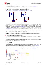
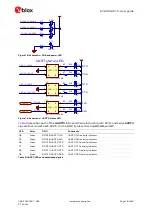
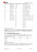
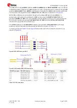
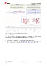
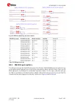
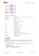
The
JTAG
interface of the
IRIS-W10
module is connected to
J20 and FTDI
chip through
resistors, and pin headers simultaneously by default, as shown in
and
should be set to their default connections, as
shown in
Figure 23: RF-CNTRL strap-in SW8
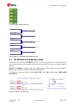
Figure 24: IRIS module SWD/JTAG connection
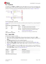
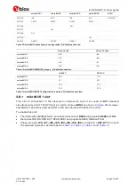
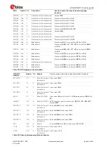
IRIS-W10 pin name
IRIS-W10 function
Resistor/Jumper
Interface IC function
Header/Pin
A14
GPIO7/JTAG-TMS
R5/J34
FTDI-
JTAG-TMS, Pin 19
J70/3
B14
GPIO6/JTAG-TCK
R1/J15
FTDI-JTAG-TCK, Pin 16
J10/3
A12
GPIO9/JTAG-TDO
R4/J36
FTDI-
JTAG-TDO, Pin 18
J70/4
B12
GPIO8/JTAG-TDI
R3/J35
FTDI-
JTAG-TDI, Pin 17
J10/4
B11
GPIO10/JTAG-RESETn
R6/J37
FTDI-
JTAG-RESETn, Pin 22
J47/8
Table 10: JTAG connections


