EVK-7 / EVK-8 / EVK-M8 User Guide
UBX-14002502 - R09
Early Production Information
Device description
Page 12 of 28
4.3.5
RST button
The RST button on the front panel resets the unit. To avoid an inadvertent reset, the button is recessed.
4.3.6
Safe boot button
This is used to set the unit in safe boot mode. In this mode the receiver executes only the minimal functionality,
such as updating new firmware into the SQI flash. In order to set the receiver in safe boot mode please follow
these steps.
1.
Press the BOOT button and keep holding
2.
Press the RST button
3.
Release the RST button
4.
Release the BOOT button
5.
If the UART interface has to be used, the training sequence has to be sent to the receiver.
The training sequence is a transmission of 0x55 55 at the baud rate of 9600 Bd. Wait for at least 100
milliseconds before the interface is ready to accept commands.
4.3.7
Slide Switch
Use the slide switch on the front panel to choose between I2C (and UART) and SPI
communication ports. You
must reset the unit by pressing the RST button when the slide switch has been changed.
1.
I2C
– In this selection the EVK operates with the UART (RS232 DB9 – rear panel or the 3.3 V level TxD
(MISO), RxD (MOSI) at the front panel). Also the communication via 3.3 V DDC interface (I2C) is
selected.
2.
SPI –
In this selection the EVK operates only with the SPI interface. RS232 (DB9) is switched off.
4.3.8
Test Connector
This 14-pin test-connector provides additional functionality to the EVK, allowing access to the interface pins and
an ability to measure the current used by the EVK. All pins are ESD protected.
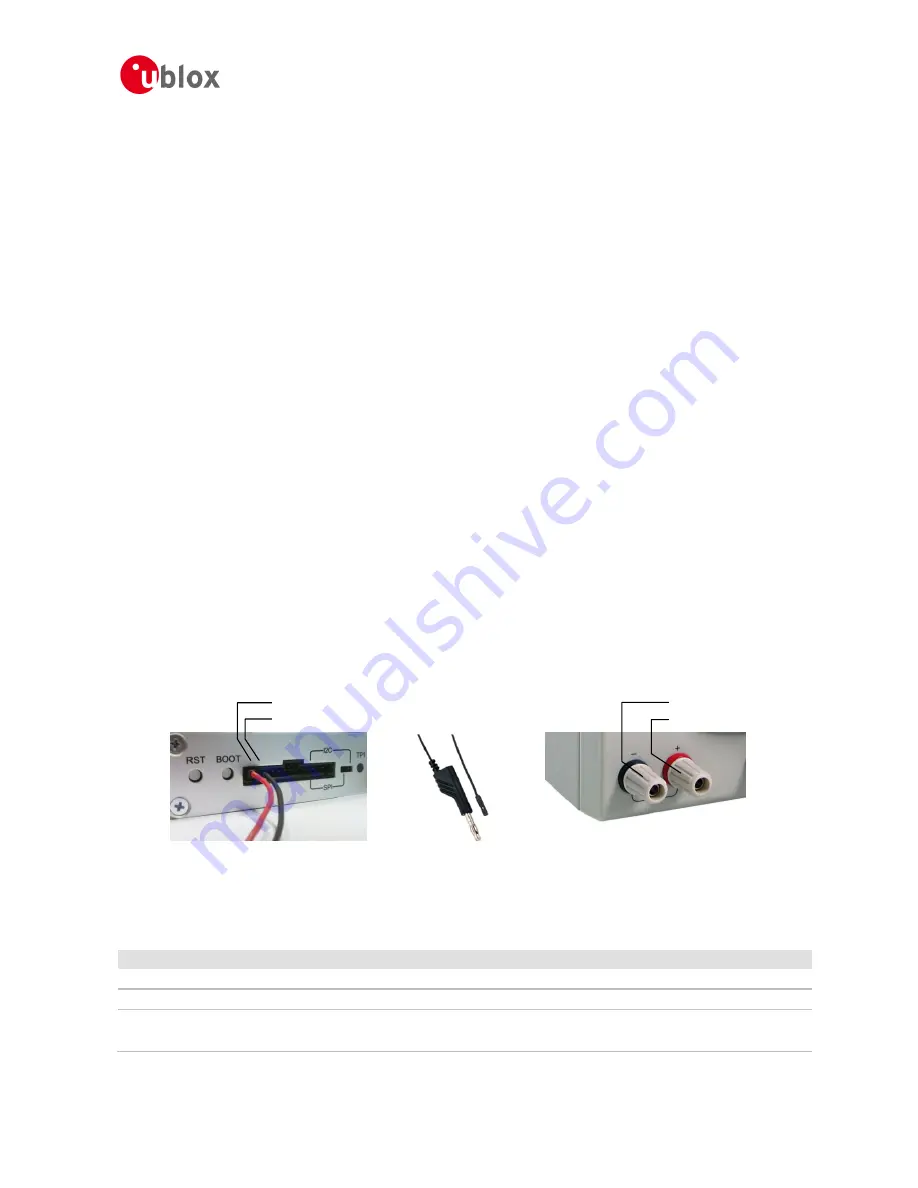
For accurate measurements, it is recommended to use a cable of at most 1 meter in length. Figure 4 shows an
example of a power supply connected to the test connector by using standard adapter cables from the
manufacture Hirschmann. Figure 5 shows an example for overall current measurement. When connecting the
3.3 V digital interfaces RS232, SPI and DDC to your application, a cable length less than 25 cm is recommended.
PIN Nr.:
PIN NAME
I/O
LEVEL
DESCRIPTION
14
V5_IN
I
4.75 V – 5.25 V
Power input – can be used instead of USB
13
GND
I
-
Common ground pin
12
P1A (VCC)
O
3.3 V
Power output – max. current supply 100 mA
1
Ω
1% resistor for over-all current measurement to pin 11 (P1B)
NOTE: the current includes also SQI Flash, LNA
Figure 4: Example 5V DC power supply
V5_IN
GND
GND
V5_IN
Hirschmann
Part Nr.: 934160100


