


SARA-G3 series - System Integration Manual
UBX-13000995 - R06
Objective Specification
Design-in
Page 118 of 218
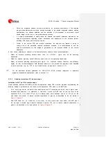
2.3.2
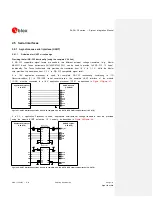
Antenna detection interface (ANT_DET)
2.3.2.1
Guidelines for ANT_DET circuit design
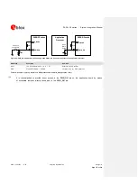
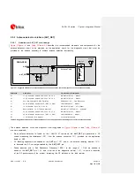
describe the recommended schematic and components for the
antenna detection circuit to be provided on the application board for the diagnostic circuit that must be
provided on the antenna assembly to achieve antenna detection functionality.
Application Board
Antenna Cable
SARA-G350
56
ANT
62
ANT_DET
R1
C1
D1
L1
C2
J1
Z
0
= 50 ohm
Z
0
= 50 ohm
Z
0
= 50 ohm
Antenna Assembly
R2
C3
L2
Radiating
Element
Diagnostic
Circuit
Figure 41: Suggested schematic for antenna detection circuit on application board and diagnostic circuit on antenna assembly
Reference
Description
Part Number - Manufacturer
C1
27 pF Capacitor Ceramic C0G 0402 5% 50 V
GRM1555C1H270J - Murata
C2
33 pF Capacitor Ceramic C0G 0402 5% 50 V
GRM1555C1H330J - Murata
D1
Very Low Capacitance ESD Protection
PESD0402-140 - Tyco Electronics
L1
68 nH Multilayer Inductor 0402 (SRF ~1 GHz)
LQG15HS68NJ02 - Murata
R1
10 k
Resistor 0402 1% 0.063 W
RK73H1ETTP1002F - KOA Speer
J1
SMA Connector 50
Through Hole Jack
SMA6251A1-3GT50G-50 - Amphenol
C3
22 pF Capacitor Ceramic C0G 0402 5% 25 V
GRM1555C1H220J - Murata
L2
68 nH Multilayer Inductor 0402 (SRF ~1 GHz)
LQG15HS68NJ02 - Murata
R2
15 k
Resistor for Diagnostic
Various Manufacturers
Table 22: Suggested components for antenna detection circuit on application board and diagnostic circuit on antenna assembly
The antenna detection circuit and diagnostic circuit suggested in
are here explained:
When antenna detection is forced by the +UANTR AT command, the
ANT_DET
pin generates a DC
current measuring the resistance (R2) from the antenna connector (J1) provided on the application
board to GND
DC blocking capacitors are needed at the
ANT
pin (C2) and at the antenna radiating element (C3)
to decouple the DC current generated by the
ANT_DET
pin
Choke inductors with a Self Resonance Frequency (SRF) in the range of 1 GHz are needed in
series at the
ANT_DET
pin (L1) and in series at the diagnostic resistor (L2), to avoid a reduction
of the RF performance of the system, improving the RF isolation of the load resistor.