background image


LILY-W1 series - System integration manual 

UBX-15027600 - R09 

System description


Page 6 of 64 

C1 - Public 


1


System description 

1.1


Overview and applications 

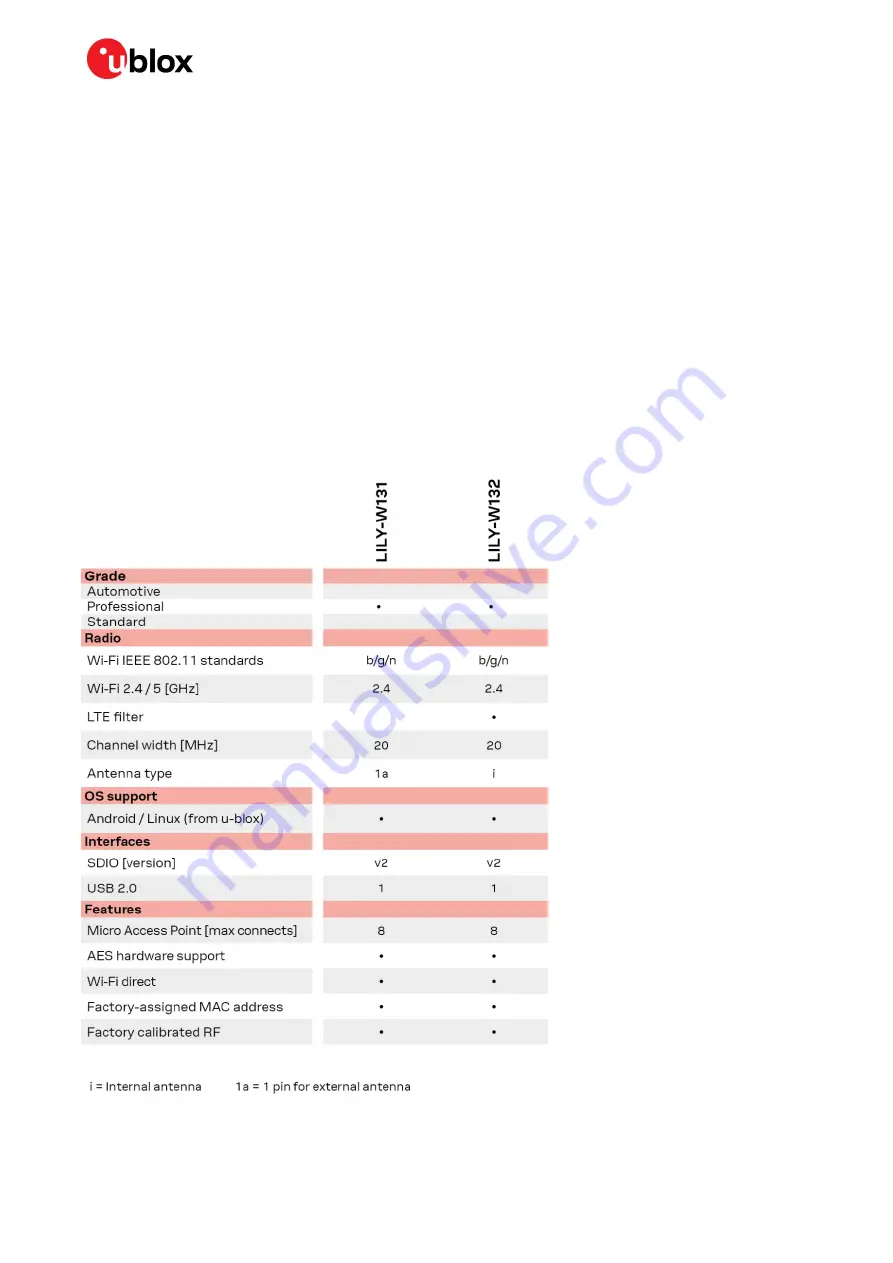
The LILY-W1 series modules are ultra-compact Wi-Fi front end modules that include variants with or 
without an internal antenna and LTE filter to enable in-device co-existence without jeopardizing Wi-
Fi performance. They are designed for integration with an LTE radio application. LILY-W1 supports 
IEEE 802.11b/g/n standards. The modules include an integrated MAC/Baseband processor, RF front-
end components and band pass filter. The LILY-W132 with internal antenna includes a BAW filter 
specially designed for optimal LTE and Wi-Fi coexistence applications. The modules are developed for 
reliable, high demanding industrial devices and applications and deliver high performance 
connectivity. 

The modules are radio type approved for Europe (ETSI RED), US (FCC CFR 47 part 15 unlicensed 
modular transmitter approval), Canada (ISEDC RSS), Taiwan (NCC), and Japan (Giteki). The main 
features and interfaces of LILY-W1 series are summarized in Table 1.


Table 1: Key features of LILY-W1 series 

Содержание LILY-W1 Series

Страница 1: ...ased modules are ultra compact cost efficient IEEE 802 11b g n Wi Fi front end modules in the LILY form factor This module series includes variants with or without internal antenna and LTE filter It includes an integrated MAC Baseband processor and RF front end components It can connect to a host through its SDIO or USB interface www u blox com UBX 15027600 R09 ...

Страница 2: ...fication This document applies to the following products Product name Type number Firmware version PCN reference Product status LILY W131 LILY W131 00B 00 SDIO driver Package SD UAPSTA 8801 FC18 MMC 14 85 36 p101 C3X14160_B0 GPL Firmware version 14 85 36 p101 USB driver Package USB UAPSTA 8801 FC18 X86 14 85 36 p101 C3X14160_B0 GPL Firmware version 14 85 36 p101 N A Mass Production LILY W132 LILY ...

Страница 3: ...ls 12 1 4 4 Configuration signals 12 1 5 Data communication interfaces 12 1 5 1 SDIO interface 12 1 5 2 USB 2 0 interface 13 1 6 Antenna interfaces 14 1 6 1 Approved antenna designs 14 1 7 Other remarks 14 1 7 1 Unused pins 14 2 Design in 15 2 1 Overview 15 2 2 Antenna interface 15 2 2 1 RF transmission line design LILY W131 only 16 2 2 2 Antenna design LILY W131 only 17 2 2 3 On board antenna des...

Страница 4: ...ading the drivers 35 3 6 1 SDIO driver 35 3 6 2 USB driver 36 3 6 3 Unloading the drivers 37 3 7 Reserving MAC addresses 37 3 8 Prevent high current in deep sleep 38 3 9 Configuration of transmit power limits 38 3 9 1 Purpose 38 3 9 2 Transmit power limit configuration file format 38 3 9 3 Applying the transmit power limit configuration 39 3 10Adaptivity configuration Energy Detection 40 3 11Usage...

Страница 5: ...pliance 50 5 3 1 Safety standard 50 5 3 2 CE Equipment classes 50 5 4 NCC end product regulatory compliance 50 5 4 1 Modular transmitter requirements 51 5 4 2 End product labeling requirements 51 5 5 Japan End product regulatory compliance 51 6 Product testing 53 6 1 u blox in series production test 53 6 2 OEM manufacturer production test 53 6 2 1 Go No go tests for integrated devices 54 6 2 2 RF ...

Страница 6: ...1b g n standards The modules include an integrated MAC Baseband processor RF front end components and band pass filter The LILY W132 with internal antenna includes a BAW filter specially designed for optimal LTE and Wi Fi coexistence applications The modules are developed for reliable high demanding industrial devices and applications and deliver high performance connectivity The modules are radio...

Страница 7: ...ed LILY W132 Single stream with an internal PIFA antenna and LTE filter 1 1 3 Operation modes The LILY W1 series modules have several operation modes which are defined in Table 2 along with related guidelines General Status Operating Mode Description Power down Not Powered VCC and VCC_IO supply not present or below the operating range module is switched off Power Down VCC and VCC_IO supply within ...

Страница 8: ...ready to receive packets but is not actively decoding any because none are being transmitted to it Active Tx Rx data connection enabled and system runs at specified power consumption Table 2 Description of operation modes for LILY W1 series 1 2 Pin configuration and function 1 2 1 Pin attributes The pin attributes described in Table 3 are 1 Function Pin function 2 Pin name The name of the package ...

Страница 9: ...ck input SDIO 1 bit Mode Clock input SDIO SPI Mode Clock input SDIO_CMD USB_VBUS_ON 4 VCC_IO I O SDIO Command SDIO 4 bit Mode Command response SDIO 1 bit Mode Command line SDIO SPI Mode Data input USB Mode USB_VBUS_ON SDIO_D0 3 VCC_IO I O SDIO data 0 SDIO 4 bit Mode Data line Bit 0 SDIO 1 bit Mode Data line SDIO SPI Mode Data output SDIO_D1 1 VCC_IO I O SDIO data 1 DIO 4 bit Mode Data line Bit 1 S...

Страница 10: ...C through internal LDOs The current drawn by the LILY W1 series through the VCC pins can vary by several orders of magnitude depending on operation mode and state It can change from the high current consumption during Wi Fi transmission at maximum RF power level in connected mode to the low current consumption during low power idle mode with the power saving configuration enabled Detailed descript...

Страница 11: ... is recommended to apply 1 ms delay with respect to VCC VCC_IO ramp up Otherwise the PD n can be left open in this case the module will handle power on sequence by itself During power up of the LILY W1 series module it is a good practice to enable VCC first followed by VCC_IO shortly after to reduce the inrush current from the main supply It is suggested that the PD n is held low during start up a...

Страница 12: ...mmunication busses configuration and host side drivers USB mode USB SDIO n pin not connected Commands and data regarding Wi Fi traffic will be transferred via the USB bus SDIO mode USB SDIO n pin grounded Commands and data regarding Wi Fi traffic will be transferred via the SDIO bus The designer must guarantee that the pin is properly set before the PD n release Name I O Description Remarks USB SD...

Страница 13: ...t 3 External PU required Table 8 SDIO signal definition The module s SDIO host interface pins are powered by the VCC_IO voltage domain 1 5 2 USB 2 0 interface The USB device interface is compliant with the USB 2 0 Specification 6 The main features of the USB interface are High Full speed operation 480 12 Mbps Suspend host resume device resume remote wake up Built in DMA engine to reduce interrupt ...

Страница 14: ...ided between the various antennas in the system Special care should be taken to maximize isolation between antennas operating in the same or nearby bands See section 2 2 for information on how to properly design circuits that are compliant with these requirements 1 6 1 Approved antenna designs LILY W1 modules come with a pre certified design that can be used to save costs and time during the certi...

Страница 15: ...pliance with regulatory standards for radiated emissions Follow the recommendations provided in section 2 4 for schematic and layout design System functions PD n and pins indicated as Configuration signals Accurate design is required to guarantee that the voltage level is well defined during module boot Follow the recommendations provided in section 2 6 for schematic and layout design Other pins s...

Страница 16: ...ssion line trace design To properly design a 50 Ω transmission line the following remarks should be taken into account The designer should provide enough clearance from surrounding traces and ground in the same layer in general a trace to ground clearance of at least two times the trace width should be considered and the transmission line should be guarded by ground plane area on each side The cha...

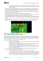
Страница 17: ...re 5 Example of RF trace and ground design from LILY W1 Evaluation Kit EVK 2 2 2 Antenna design LILY W131 only Designers must take care of the antennas from all perspective at the very start of the design phase when the physical dimensions of the application board are under analysis decision since the RF compliance of the device integrating LILY W1 module with all the applicable required certifica...

Страница 18: ...ss or the S11 as the VSWR refers to the amount of reflected power measuring how well the primary antenna RF connection matches the 50 Ω characteristic impedance of the ANT pin The impedance of the antenna termination must match as much as possible the 50 Ω nominal impedance of the ANT pin over the operating frequency range maximizing the amount of the power transferred to the antenna Efficiency 1 ...

Страница 19: ...es used in the design Table 12 suggests some RF connector plugs that can be used by the designers to connect RF coaxial cables based on the declaration of the respective manufacturers The Hirose U FL R SMT RF receptacles or similar parts require a suitable mated RF plug from the same connector series Due to wide usage of this connector several manufacturers offer compatible equivalents Manufacture...

Страница 20: ...egrated antenna requirements The ground plane of the application PCB may be reduced down to a minimum size that must be similar to one quarter of wavelength of the minimum frequency that has to be radiated however overall antenna efficiency may benefit from larger ground planes Proper placement of the antenna and its surroundings is also critical for antenna performance Avoid placing the antenna c...

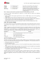
Страница 21: ...als from LILY W131 the suggested parts for switch and filtering are provided in Table 14 The designers should follow those recommendations when including an RF switch in their design ANT_SEL and ANT_SEL n are hardware controlled and have inverted logic Isolation between the two antennas should be maximized See Table 11 for the specific requirements The trace impedance from ANT pin through the SPDT...

Страница 22: ... ground pins to solid ground on the application board as a good low impedance connection to external ground can minimize power loss and improve RF and thermal performance LILY W1 modules must be sourced through VCC and VCC_IO pins with proper DC power supplies that comply with the requirements summarized in Table 4 Good connection of the LILY W1 series module power supply pins with DC supply sourc...

Страница 23: ...M PFM mode can be used provided that the PFM PWM modes and transition between modes complies with the requirements 2 3 1 2 Guidelines for supply circuit design using a Low Drop Out LDO linear regulator The use of a linear regulator is suggested when the difference from the available supply rail and the VCC or VCC_IO value is relatively low The linear regulators provide acceptable efficiency when t...

Страница 24: ... clock input pin and can be assembled only for EMI purpose The capacitor value adds to total line capacitance and must not exceed total allowed capacitance to avoid violation of clock rise and fall timing specifications Signal Group Parameter Min Typ Max Unit CLK CMD DAT 0 3 Single ended impedance 𝑍𝑍0 50 Ω CLK CMD DAT 0 3 Impedance control 𝑍𝑍0 10 𝑍𝑍0 𝑍𝑍0 10 Ω DAT 0 3 Pull Up range Rdat 10 47 100 k...

Страница 25: ...they cause signal degradation More details about proper selection of ESD protections can be found in section 2 9 2 5 Other interfaces and notes All pins have internal keeper resistors leave it open if not used 2 6 General high speed layout guidelines These general design guidelines are considered as best practices and are valid for any bus present in the LILY W1 modules The designer should priorit...

Страница 26: ... board No digital routing is allowed in the GND reference plane area of RF traces ANT pin and Antenna Is strongly recommended to avoid digital routing beneath all layers of RF traces Ground cuts or separation are not allowed below the module Minimize the length of the RF traces as first priority Then minimize bus length to reduce potential EMI issues from digital busses All traces Including low sp...

Страница 27: ...or LILY W1 module The exact mask geometries distances and stencil thicknesses must be adapted to the specific production process of the customer 2 8 Thermal guidelines The LILY W1 series modules have been successfully tested from 40 C to 85 C ambient temperature The board will generate heat during high loads that must be dissipated to sustain the lifetime of the components The improvement of the m...

Страница 28: ...stated in Table 17 Applicability Immunity level All pins except ANT Human Body Model HBM ANSA ESDA JEDEC JS 001 2014 2000 V Charged Device Model CDM JESD22 C101 500 V ANT pin and Internal antenna Human Body Model HBM ANSA ESDA JEDEC JS 001 2014 300 V Charged Device Model CDM JESD22 C101 600 V Table 17 ESD immunity rating for pins of LILY W1 module The designer must implement proper measures to pro...

Страница 29: ...final matching RF co location additional filters have been considered in the design 2 10 2 Layout checklist PCB stack up and controlled impedance traces follow PCB manufacturer s recommendation All pins are properly connected and the package follows u blox s recommendations for pin design Proper clearance has been provided between RF section and digital section Proper isolation has been provided b...

Страница 30: ...rms We recommended that you use the latest available host interface driver version and port this to the used operating system version The Software section of this manual describes only the NXP reference drivers which can be obtained through u blox support The mwifiex open source drivers that are distributed with the Linux kernel are not officially supported by u blox For a list of the supported dr...

Страница 31: ...ure where the Wi Fi firmware handles all 802 11 MAC management tasks Figure 11 shows the basic driver and firmware architecture The following steps are performed while loading the Wi Fi host driver The driver registers itself with the MMC SDIO or USB bus driver Upon successful registration the bus driver calls the Wi Fi driver s probe handler when the module is detected The probe handler allocates...

Страница 32: ... the USB stack of the Linux kernel thus the respective stack must be enabled on the target system For configuration the Linux reference driver supports the following two driver API options The old Linux wireless extensions WEXT interface The new cfg80211 configuration API To enable these APIs on the target system the following must be selected in the kernel configuration CONFIG_WIRELESS_EXT cannot...

Страница 33: ...re a full kernel build must be executed to make the module versioning work 3 4 4 2 Wi Fi driver and tools To compile the Wi Fi drivers and tools go to the driver packages s wlan_src subdirectory and run make build For cross compilation you should specify the target architecture cross toolchain prefix and the directory with the kernel sources used to build the kernel on the target system that is Fw...

Страница 34: ... the application binaries to an appropriate location on the target file system and add it to the PATH environment variable if required 2 The kernel modules should be copied to somewhere below the modules directory of the kernel for example lib modules 3 19 8 updates Run the depmod command afterwards to update the module dependencies and to have the modules findable by the modprobe utility 3 Copy t...

Страница 35: ...nstalled correctly you can load them by simply issuing the following command Else you have to load them separately using the insmod command This will automatically load the sd8801 kernel module and all its dependencies such as mlan or cfg80211 The cfg80211_wext 0xf module parameter in the above mentioned example informs the driver to enable support for the wireless extensions interface and for the...

Страница 36: ...mand If the drivers are successfully loaded you should see them in the list of loaded modules as shown below via lsmod command The internal name for the usb8801 module is usb8xxx When the module is detected on the USB interface the driver will automatically download the firmware to it initialize the hardware and register the network interfaces wlan Loading MWLAN driver wlan Driver loaded successfu...

Страница 37: ...nge the init_cfg conf file as per the requirements and also make sure that each interface is assigned a wlan Loading MWLAN driver usbcore registered new interface driver usb8xxx wlan Driver loaded successfully usb 2 1 new high speed USB device number 4 using musb hdrc Request firmware mrvl usb8801_uapsta_usb bin WLAN FW is downloaded usb_reset_device successful usb 2 1 USB disconnect device number...

Страница 38: ... depend on the following Regulatory domain limits Gain of the antenna and antenna trace design A configuration file on the host system is used to reduce the transmit power levels as needed Transmit power limit configuration files for the reference design Appendix B and the approved antennas are provided by u blox for each of the certified regulatory domains The correct transmit power limits must b...

Страница 39: ...igures the following transmit power limits for channel 1 in the 2 4 GHz band 16 dBm for 802 11b rates BPSK QPSK CCK 14 dBm for 802 11g OFDM 6 54 Mbps 13 dBm for 802 11n HT20 MCS 0 7 3 9 3 Applying the transmit power limit configuration The configuration file txpwrlimit_cfg conf contains a section for setting the transmit power limits for the 2 4 band This can be applied using the mlanutl tool as s...

Страница 40: ... 300 328 standard for the offset of 0x1b Changes to the antenna path of the reference design such as introducing a higher attenuation on the antenna path have to be reflected into the energy detection configuration file Thus the offset can be increased to compensate the additional attenuation of the antenna path where increasing the value of the offset would result in a more sensitive behavior Inc...

Страница 41: ... and the proc file system The driver states are recorded and can be retrieved through the proc file system during runtime The following files containing the debug information are provided the actual location is dependent on the Linux kernel version proc mwlan config or proc net mwlan config proc mwlan mlanX info or proc net mwlan mlanX info proc mwlan mlanX debug or proc net mwlan mlanX debug mlan...

Страница 42: ...bg parameter The value of drvdbg can be given as a module parameter when the driver is loaded by writing to the proc file system s debug file or by setting it via the iwpriv or mlanutl tool Listing 8 Debug examples bit 0 MMSG PRINTM MMSG bit 1 MFATAL PRINTM MFATAL bit 2 MERROR PRINTM MERROR bit 3 MDATA PRINTM MDATA bit 4 MCMND PRINTM MCMND bit 5 MEVENT PRINTM MEVENT bit 6 MINTR PRINTM MINTR bit 7 ...

Страница 43: ...GND i e the work table and the PCB GND then the first point of contact when handling the PCB must always be between the local GND and PCB GND Before mounting an antenna patch connect ground of the device When handling the RF pin do not come into contact with any charged capacitors and be careful when contacting materials that can develop charges e g patch antenna 10 pF coax cable 50 80 pF m solder...

Страница 44: ...up rate to TSMIN K s 3 TSMIN C 150 TSMAX C 200 tS from 25 C s 150 tS Pre heat s 110 Peak TL C 217 tL time above TL s 90 TP absolute max C 260 tP time above TP 5 C s 40 Cooling Ramp down from TL K s 6 General Tto peak s 300 Allowed soldering cycles 1 Table 24 Recommended reflow profile Figure 12 Reflow profile Lower value of TP and slower ramp down rate 2 3 C sec is preferred After reflow soldering...

Страница 45: ...hole technology THT components and surface mount technology SMT devices may require wave soldering to solder the THT components Only a single wave soldering process is allowed for boards populated with the modules Miniature Wave Selective Solder process is preferred over traditional wave soldering process Hand soldering is not recommended Rework is not recommended Conformal coating may affect the ...

Страница 46: ...nas In the end product the LILY W1 series module must be installed in such a way that only authorized antennas can be used The end product must use the antenna trace reference design described in Appendix B Any notification to the end user about how to install or remove the integrated radio module is NOT allowed If these conditions cannot be met or any of the operating instructions are violated th...

Страница 47: ...ox FCC ISED certification ID If the conditions in sections 5 1 General requirements 5 2 FCC ISED End product regulatory compliance and all sub sections from 5 2 3 are met the u blox modular FCC ISED regulatory authorization is valid Only under the circumstances may the end product refer to the u blox FCC ID and ISED certification number u blox may be able to support updates to the u blox regulator...

Страница 48: ...ith less or same gain as an already approved antenna can be added under a Class I Permissive Change Antenna trace designs deviating from the u blox reference design and new antenna types are added under a Class II Permissive Change Integrators that intend to refer to the u blox FCC ID ISED certification ID must contact their local support team to discuss the Permissive Change Process For contact i...

Страница 49: ...d on an exterior surface of the end product such that it will be visible upon inspection in compliance with the modular labeling requirements of OET KDB 784748 The host user manual must also contain clear instructions on how end users can find and or access the FCC ID of the end product In compliance with the modular labeling requirements of OET KDB 784748 the label on the LILY W1 series module th...

Страница 50: ...ies Data Sheet 1 5 3 CE End product regulatory compliance 5 3 1 Safety standard In order to fulfill the safety standard EN 60950 1 11 the LILY W1 series module must be supplied with a Class 2 Limited Power Source 5 3 2 CE Equipment classes This module operates as Class 1 radio equipment The End product that utilizes the LILY W1 series module inherits the equipment class of the module Class 1 radio...

Страница 51: ...el usage under NCC regulation Refer to the power tables in Appendix C for maximum configuration settings in the Taiwan regulatory domain For information about the approved antennas for LILY W1 series refer to the LILY W1 series Data sheet 1 5 4 1 Modular transmitter requirements The end product is required either to integrate one of the antennas which is approved with the module for use in Taiwan ...

Страница 52: ...1 series in Wi Fi mode in Japan Channel number Channel center frequency MHz Indoor use allowed Outdoor use allowed Modulation type Max EIRP 1 13 2412 2472 Yes Yes 802 11b 3 00 mW MHz 1 13 2412 2472 Yes Yes 802 11g 1 50 mW MHz 1 13 2412 2472 Yes Yes 802 11n HT20 1 50 mW MHz Table 28 Channel usage restrictions in Japan The end product technical documentation shall include a copy of the Japan Radio C...

Страница 53: ...erface communication Digital I O tests Measurement and calibration of RF characteristics in all supported bands such as frequency tuning of reference clock calibration of transmitter power levels etc Verification of RF characteristics after calibration that is modulation accuracy power levels spectrum etc are checked to ensure they are all within tolerances when calibration parameters are applied ...

Страница 54: ... provided in the NXP driver package for details on the usage of the tools Example commands that can be used to get the signal quality are iw dev mlan0 link for station mode iw dev uap0 station get peer MAC address for AP mode A very simple test can be performed by just scanning for a known AP on a specific frequency and checking the signal level for example iw dev mlan0 scan freq freq These kinds ...

Страница 55: ...tter and receiver power levels to check component assembly related to the module antenna interface and to check other device interfaces that affect the RF performance The module can also be set into TX test modes without using the labtool utility Sample scripts for this can be provided through u blox support The test modes for Wi Fi still require the use of the manufacturing firmware To avoid modu...

Страница 56: ...stitute of Electrical and Electronics Engineers KDB Knowledge database LDO Low drop out LPM Link power management LTE Long Term Evolution MAC Medium access control MMC MultiMedia card NSMD Non solder mask defined OEM Original equipment manufacturer OET Office of Engineering and Technology OTP One time programmable OS Operating system PCB Printed circuit board RF Radio frequency RIFS Reduced inter ...

Страница 57: ...ntegration manual UBX 15027600 R09 Appendix Page 57 of 64 C1 Public Abbreviation Definition WFD Wi Fi Direct WLAN Wireless local area network WPA Wi Fi Protected Access Table 29 Explanation of the abbreviations and terms used ...

Страница 58: ...B layout must be identical to the one provided by u blox please implement one of the reference designs included in this annex or contact u blox The designer must use the stack up provided by u blox RF traces on the main PCB are part of the certified design The available designs are presented in this annexure B 1 Reference design for external antennas U FL connector When using the LILY W131 togethe...

Страница 59: ...nna 3 Antenna coplanar microstrip matched to 50 Ω 4 Top layer GND plane 5 Host PCB Should have a solid GND inner layer under and around the RF components vias and small openings is allowed 6 10pF COG 0402 10P 0 25P 25V Antenna connector capacitor Table 31 Included part in the antenna connector reference design B 1 2 PCB stack up The stack up from top to solid GND layer used in the reference design...

Страница 60: ...µm εr 4 Table 33 Coplanar micro strip specification B 1 4 Mechanical dimensions The mechanical dimensions and position of the components are specified in Figure 20 The solid GND layer beneath the top layer shall be minimum 19x15 mm according Figure 20 No traces are allowed to be routed on the GND layer within this area but vias and small openings are allowed The minimum size of the top layer GND p...

Страница 61: ...the module is used The antenna gain has to be added for EIRP figures Approval Module Modulation Channel Power dBm 1 2 10 11 12 13 ETSI All 802 11b 14 14 14 14 802 11g n 16 16 16 16 FCC ISED All 802 11b 16 16 16 802 11g 14 16 13 802 11n 13 16 11 Japan MIC All 802 11b g n 16 16 16 16 Taiwan NCC LILY W131 802 11b g n 16 16 16 LILY W132 802 11b 14 16 16 802 11g n 15 16 16 Table 34 Maximum allowed cond...

Страница 62: ... Matters ERM ElectroMagnetic Compatibility EMC standard for radio equipment and services Part 1 Common technical requirements 9 IEC61340 5 1 Protection of electronic devices from electrostatic phenomena General requirements 10 JEDEC J STD 020C Moisture Reflow Sensitivity Classification for Nonhermetic Solid State Surface Mount Devices 11 ETSI EN 60950 1 2006 Information technology equipment Safety...

Страница 63: ... 2 8 R04 11 Oct 2016 mzes sbia kgom Added Wi Fi Tx output power limits in Appendix C Included regulatory compliance for Japan section 5 5 R05 11 Jan 2017 sbia shoe kgom Included regulatory compliance for Taiwan section 5 4 and Appendix C Added information about how to prevent high current consumption in sleep mode section 3 7 Replaced Document status with Disclosure restriction on page 2 R06 10 Ap...

Страница 64: ...x com Regional Office China Beijing Phone 86 10 68 133 545 E mail info_cn u blox com Support support_cn u blox com Regional Office China Chongqing Phone 86 23 6815 1588 E mail info_cn u blox com Support support_cn u blox com Regional Office China Shanghai Phone 86 21 6090 4832 E mail info_cn u blox com Support support_cn u blox com Regional Office China Shenzhen Phone 86 755 8627 1083 E mail info_...

Отзывы: