LEA-5, NEO-5, TIM-5H - Hardware Integration Manual
GPS.G5-MS5-09027-A2
Released
Hardware description
Page 13 of 68
1.5.3
DDC (LEA-5, NEO-5)
An I
2
C compatible Display Data Channel (DDC) interface is available with LEA-5 and NEO-5 modules for serial
communication. For more information about DDC implementation refer to the
u-blox 5 Receiver Description
including Protocol Specification [2].
u-blox 5 GPS receivers normally run in the slave mode. Master Mode is only supported when external
EEPROM is used to store configuration. No other nodes are connected to the bus. In this case, the
receiver attempts to establish presence of such a non-volatile memory component by writing and
reading from a specific location.
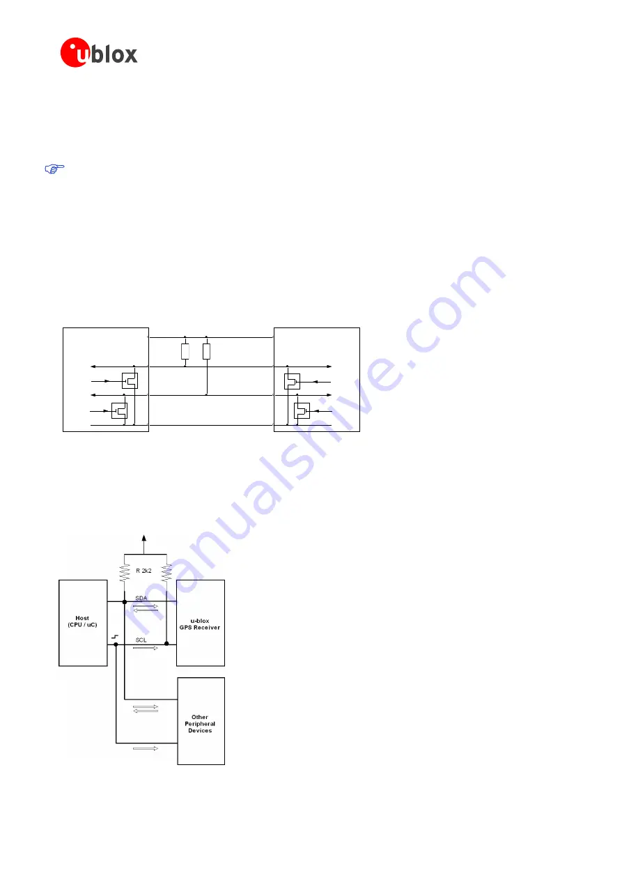
Two wires, serial data (SDA) and serial clock (SCL), carry information between the devices connected to the bus.
These lines are connected to all devices on the DDC. SCL is used to synchronize data transfers and SDA is the
data line. Both SCL and SDA lines are "o“en drain" ”rivers. This means that DDC devices can only drive them
low or leave them open. The
pull-up resistor (Rp) pulls the line up to V
DD
if no DDC device is pulling it down to
GND. If the pull-up resistors are missing, the SCL and SDA lines –are undefined and the DDC bus will not work.
For most DDC systems the low and high input voltage level thresholds of SDA and SCL depend on V
DD
. See
receiver datasheet for the applicable voltage levels.
DDC Device A
DDC Device B
V
DD
SDA
SCL
GND
Rp
Rp
SDA in
SDA out
SCL in
SDA out
SDA in
SDA out
SCL in
SDA out
Figure 4: A simple DDC connection
The signal shape and the maximum rate in which data can be transferred over SDA and SCL is limited by the
values of Rp and the wire and I/O capacitance (Cp). Long wires and a large number of devices on the bus
increase Cp, therefore DDC connections should always be as short as possible. The resistance of the pull-up
resistors and the capacitance of the wires should be carefully chosen.
Figure 5: DDC block diagram


