User's Manual l MBa8Xx UM 0100 l © 2020, TQ-Systems GmbH
Page 44
Input protection (continued)
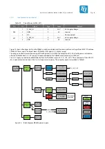
Table 49:
Pinout Power-In (X26, X27)
Pin
Pin
Signal
Type
Level
Remark
X26
1
V_24V_IN
P
24 V
24 V supply voltage
2
GND
P
0 V
Ground
3
NC
–
–
Not connected
X27
1
V_24V_IN
P
24 V
24 V supply voltage
2
GND
P
0 V
Ground
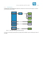
Figure 22 shows all voltages (rails) on the MBa8Xx, which are divided into three main paths consisting of two LM25119 and one
TPS45335. These supply the largest loads. (TQMa8Xx, USB supply, 12 V display supply.)
The design also allows power sequencing of all voltage levels used. With the exception of V_3V3, all voltages are switched on
after the TQMa8Xx boots. A 1.8 V supply is already provided by the TQMa8Xx and delivers up to 1000 mA.
The 1.8 V supply is provided by default directly from the TQMa8Xx via pin X2-12 (V_1V8_OUT). The second part of the LM25119
(#2) is optional and can be used if the 1.8 V rail requires more power. The assembly option is described in Table 51.
V_24V
(max. 4 A)
LM25119
#1
V_3V3
(max. 8 A)
V_5V
(max. 6 A)
LM25119
#2
V_5V_USB
(max. 6 A)
V_1V8
(max. 1.8 A)
AP7361C
AP7361C
LT3503
Optional
TPS54335
V_1V5_MPCIE
V_2V5_ETH
V_1V0_ETH
Buck
converter
Legend:
LDO/
Switch
V_12V
(max. 3 A)
FDC6331
V_3V3_MPCIE
PFET
TQMa8Xx
V_3V3_MB
Power-Rail
V_1V8
(max. 1 A)
AP7361C
V_1V2_DP
V_1V1_USB
(max. 1 A)
V_1V8_OUT
V_1V8_OUT
Optional
V_5V_CAN
DC/DC-
Converter
Galvanically
separated
R2S-0505
TQMa8Xx
Figure 22: Block diagram MBa8Xx power supply


