


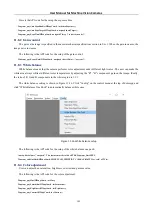
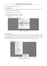


User Manual for Machine Vision Cameras
112
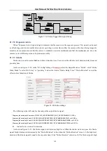
Figure 11
-
40
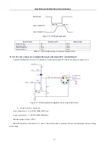
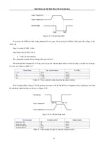
Input logic level
To prevent the GPIO pin from being damaged, first connect the ground pin GND and then input the voltage to the
Line2 pin
Input rise delay (TDR): 0.02us
Input drop delay (TDF): 0.02us
•
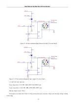
Line2 is set as output pin
The maximum current allowed through this pin is 25 mA.
When the ambient temperature is 25 degrees Celsius, the relationships between external voltage, resistance and output
low level are shown in Table 11
External voltage
Non-essential resistance
VL(GPIO)
3.3V
1KΩ
0.11V
5V
1KΩ
0.167V
12V
2.4KΩ
0.184V
24V
4.7KΩ
0.385V
Table 11
-
7
Non
-
isolated output logic low level parameters
The external pull
-
up voltage is 5V, the pull
-
up resistance is 1K Ω, the GPIO is configured as the output logic level and
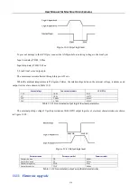
the electrical characteristics are shown in Figure 11
Figure 11
-
41
Output logic level
Parameter name
Parameter symbol
Parameter values
Output rise time
TR
0.08us
Output downtime
TF
0.02us
Output rising delay
TDR
0.1us
Output drop delay
TDF
0.04us
Table 11
-
8
Non
-
isolated output’s electrical characteristics