Toshiba Tecra 9100 Series Скачать руководство пользователя страница 247

4.8   Top Cover with Display Assembly 

4   Replacement Procedures 

4-35 


TECRA 9100 Maintenance Manual (960-347)


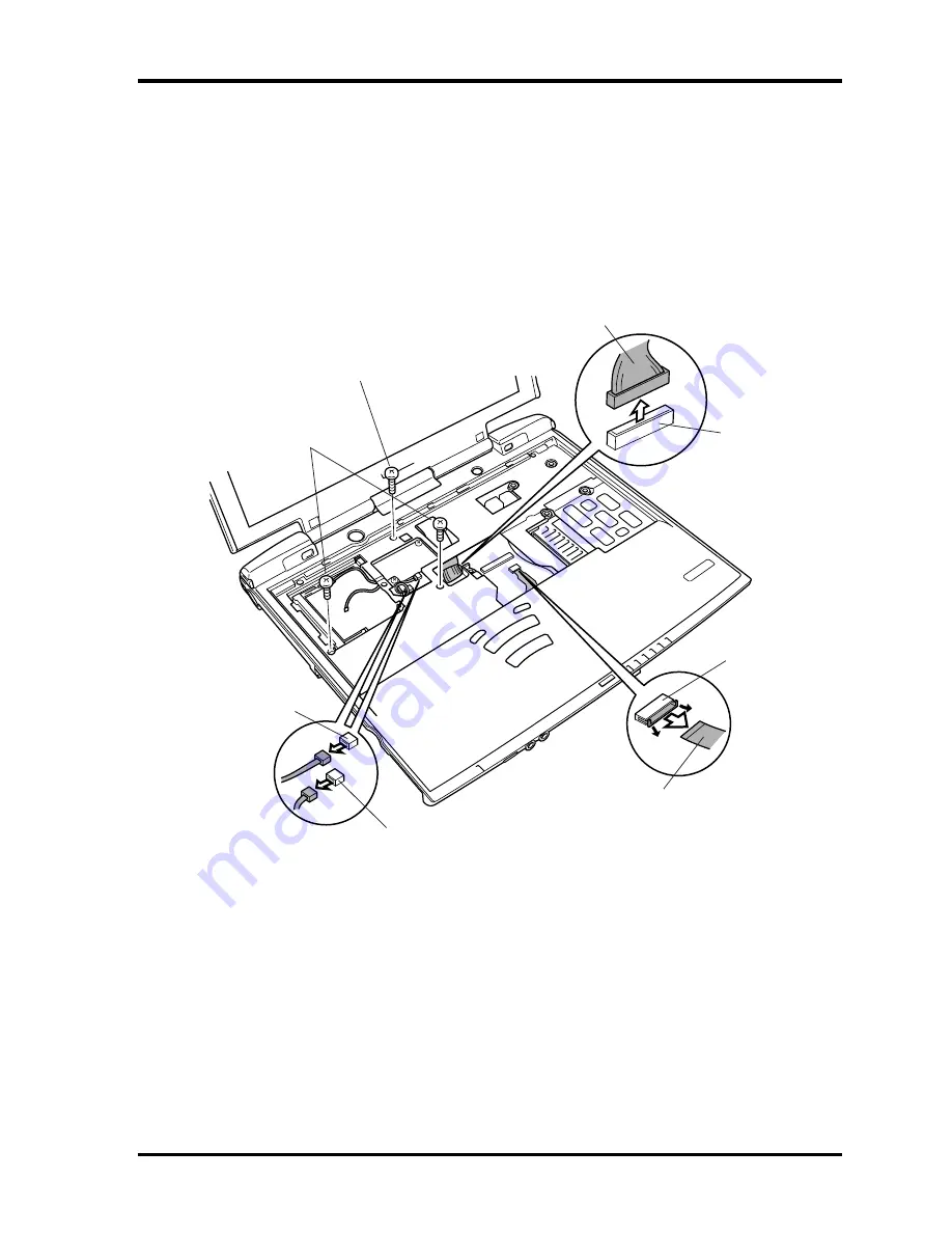
2.  Turn the computer right side up, open the display panel and disconnect the 

IPS cable


from 

PJ122

,


the 

FL/LCD cable

 from

 PJ76

 and the 

speaker cables

 from 

PJ127

 and 

PJ129

 on the 

I/O board

3. Remove 

two M2.5

×

8 screws

4. Remove 

one M2.5

×

13 black screw


M2.5

×

13 black screw

M2.5

×

8 screws

PJ76

PJ122

PJ127

LCD/FL cable

IPS cable

PJ129


Figure 4-22   Disconnecting the cables 


Содержание Tecra 9100 Series

Страница 1: ...Toshiba Personal Computer TECRA 9100 Series Maintenance Manual TOSHIBA CORPORATION File Number 960 347 ...

Страница 2: ...duction However succeeding computers and manuals are subject to change without notice Therefore Toshiba assumes no liability for damages incurred directly or indirectly from errors omissions or discrepancies between any succeeding product and this manual Trademarks IBM is a registered trademark and OS 2 and PS 2 are trademarks of IBM Corporation Microsoft MS DOS Windows DirectSound and DirectMusic...

Страница 3: ...icates the existence of a hazard that could result in bodily injury if the safety instruction is not observed CAUTION Caution indicates the existence of a hazard that could result in property damage if the safety instruction is not observed NOTE Note contains general information that relates to your safe maintenance service Improper repair of the computer may result in safety hazards Toshiba requi...

Страница 4: ...w to diagnose and resolve FRU problems Chapter 3 Test and Diagnostics describes how to perform test and diagnostic operations for maintenance service Chapter 4 Replacement Procedures describes the removal and replacement of the FRUs Appendices The appendices describe the following Handling the LCD module Board layout Pin assignments Keyboard scan character codes Key layout Wiring diagrams BIOS Rew...

Страница 5: ...n the keyboard is printed in boldface type Key operation Some operations require you to simultaneously use two or more keys We identify such operations by the key top symbols separated by a plus sign For example Ctrl Pause Break means you must hold down Ctrl and at the same time press Pause Break If three keys are used hold down the first two and at the same time press the third User input Text th...

Страница 6: ...vi TECRA 9100 Maintenance Manual 960 347 ...

Страница 7: ... Chapter 2 Troubleshooting Procedures 2 1 Troubleshooting 2 1 2 2 Troubleshooting Flowchart 2 2 2 3 Power Supply Troubleshooting 2 6 2 4 System Board Troubleshooting 2 16 2 5 FDD Troubleshooting 2 28 2 6 HDD Troubleshooting 2 31 2 7 Keyboard and PAD I F Troubleshooting 2 36 2 8 Display Troubleshooting 2 39 2 9 CD R RW Drive Troubleshooting 2 41 2 10 COMBO Drive Troubleshooting 2 43 2 11 Modem Trou...

Страница 8: ...isk Test 3 27 3 12 Real Timer Test 3 29 3 13 NDP Test 3 31 3 14 Expansion Test 3 32 3 15 CD ROM DVD ROM Test 3 34 3 16 LAN Test 3 35 3 17 Error Code and Error Status Names 3 36 3 18 Hard Disk Test Detail Status 3 39 3 19 Head Cleaning 3 41 3 20 Log Utilities 3 42 3 21 Running Test 3 44 3 22 Floppy Disk Drive Utilities 3 46 3 23 System Configuration 3 51 3 24 SETUP 3 53 3 25 Modem Test Program 3 72...

Страница 9: ...rd 4 38 4 10 Sound FIR Board 4 40 4 11 RTC Battery 4 43 4 12 Speakers 4 46 4 13 IPS Board 4 51 4 14 LED Board 4 53 4 15 I O Board 4 55 4 16 Connector Board 4 57 4 17 PC Card Slot 4 59 4 18 System Board 4 61 4 19 Cooling Fan 4 63 4 20 CPU 4 66 4 21 Display Mask 4 69 4 22 FL Inverter Board 4 72 4 23 LCD Module 4 74 4 24 Antenna Coaxial Cables 4 78 4 25 LCD FL Cable 4 84 4 26 TFT FL Model 14 1 Toshib...

Страница 10: ... 1 Appendix B Board Layout B 1 Appendix C Pin Assignments C 1 Appendix D Character Codes D 1 Appendix E Key Layout E 1 Appendix F Reliability F 1 Appendix G BIOS Rewrite Procedures G 1 Appendix H EC KBC Rewrite Procedures H 1 Appendix I Reliability I 1 Appendix J Connection for Check J 1 ...

Страница 11: ...Chapter 1 Hardware Overview ...

Страница 12: ...1 Hardware Overview 1 ii TECRA 9100 Maintenance Manual 960 347 ...

Страница 13: ...Block Diagram 1 9 1 3 3 5 inch Floppy Disk Drive USB External 1 17 1 4 2 5 inch Hard Disk Drive 1 18 1 5 CD ROM Drive 1 19 1 6 DVD ROM Drive 1 20 1 7 CD R RW Drive 1 22 1 8 COMBO Drive 1 23 1 9 Power Supply 1 24 1 10 Batteries 1 26 1 10 1 Main Battery 1 26 1 10 2 Battery Charging Control 1 27 1 10 3 RTC battery 1 28 ...

Страница 14: ...e 1 22 Figure 1 9 COMBO drive 1 23 Tables Table 1 1 3 5 inch FDD specifications 1 17 Table 1 2 2 5 inch HDD specifications 1 18 Table 1 3 CD ROM drive specifications 1 19 Table 1 4 Toshiba DVD ROM drive specifications 1 20 Table 1 4 TEAC DVD ROM drive specifications 1 21 Table 1 5 CD R RW drive specifications 1 22 Table 1 6 COMBO drive specifications 1 23 Table 1 7 Power supply output rating 1 25 ...

Страница 15: ...of the following speeds Intel Mobile Pentium 4 Processor 1 70GHz 1 30V 1 20GHz 1 20V Intel Mobile Pentium 4 Processor 1 60GHz 1 30V 1 20GHz 1 20V This processor operates at 1 30V 1 20V and 133MHz bus clock A 12KB level 1 cache memory and a 512KB level 2 cache memory are built in Chipset The 9100 Series is equipped with Brookdale M MCH M Graphics and Memory Controller Hub Brookdale M ICH3 M I O Con...

Страница 16: ...lowing formats CD DA CD ROM Photo CD Multi session and CD Extra CD Plus CD R RW Drive A full size maximum 24 speed CD ROM drive maximum 8 speed CD R writing and maximum 8 speed CD RW writing maximum 14 speed CD RW reading maximum 24 speed CD ROM CD RW reading contains an AT Attachment Packet Interface ATAPI controller and supports the following formats CD DA CD ROM CD R CD RW Photo CD Multi sessio...

Страница 17: ...hat backs up the Real Time Clock and CMOS memory Universal Serial Bus USB Two USB ports are provided They enable daisy chain connection of up to 127 USB equipped devices and 12Mbps full speed or 1 5Mbps low speed serial data transfer They are designed for easy configuration by a PnP operating system and provide hot insertion ejection capability IEEE 1394 port The computer comes with one IEEE 1394 ...

Страница 18: ...ansfer data from devices such as digital cameras and Personal Digital Assistants that use SD Card flash memory Docking interface port A 242 pin docking interface port enables connection of an optional Port Replicator 2001 It provides additional features as follows RJ 45 LAN jack RT11 Modem jack External monitor port Parallel port and Serial port PS 2 Mouse port and Keyboard port DC IN socket Secur...

Страница 19: ...O The internal modem is equipped as a modem daughter card MDC The internal modem provides capability for data and fax communication and supports ITU TV 90 For data reception it operates at 56 000bps and for data transmission it operates at 33 600bps For fax transmission it operates at 14 400bps It is also equipped with Speakerphone and TAM Telephony Answering Machine function The speed of data tra...

Страница 20: ...less LAN The Mini PCI Card for wireless LAN is compatible with other LAN systems based on Direct Sequence Spread Spectrum radio technology that complies with the IEEE 802 11 Standard Revision B It supports data transfer up to 11 Mbit s It has Frequency Channel Selection 2 4GHz and allows roaming over multiple channels The front of the computer is shown in figure 1 1 Figure 1 1 Front of the compute...

Страница 21: ...104 PJ103 PJ102 PJ100 PJ801 PJ1003 Internal Microphone PJ1002 SD Card SmartMedia PJ1005 Headphone PJ1004 External Microphone PJ52 USB 1 PJ51 TV PJ54 USB 2 PJ53 PS 2 PJ5 RTC PJ2 Bluetooth PJ76 LCD FL PJ12 SO DIMM 2 PJ1 PJ2 PJ2 PJ103 PJ1000 PJ1001 PJ19 PJ18 PJ50 PJ1 PJ126 FZNSY System Board FZNSD Sound Board FSZIS Sound Flexible Board FSZIC SD Card Flexible Board FZNCN Connector Board FZNLE LED Boar...

Страница 22: ...OM CD R RW DVD ROM COMBO 2nd HDD 2nd Battery IDE FWH 4MB BGA 421pin USB Slot x6 P1 20V P1 30V Slot 2 Slot 1 Mobile Intel Pentium IV Processor Northwood ExpansionMemory DDR SDRAM PC1600 or PC2100 128 256 512MB B3V for Common Dock RJ45 foror Common Dock 1700 MHz 1600 MHz Common Dock Reserevd P 1 25V ExpansionMemory DDR SDRAM PC1600 or PC2100 128 256 512MB 200MHz VGA A SW Bluetooth Module RJ11 for Co...

Страница 23: ...ocessor 1 60GHz Processor core speed 1 60GHz Performance Mode at 1 30V and 1 20GHz Battery Optimized Mode at 1 20V Processor bus speed 400MHz Integrated L1 cache memory 12KB instruction cache and 8KB write back data cache 4 way set associative Integrated L2 cache memory 512KB ECC protected cache data array 8 way set associative Integrated NDP Memory Two BTO CTO compatible expansion memory slots ar...

Страница 24: ...r Interrupt Controller Power Management Logic Suspend Resume Logic Low Pin count LPC Bus Controller EC KBC Super I O Firmware Hub FWH I F supports BIOS BusMasterIDE UltraDMA100 66 33 Real Time Clock Stop Clock PCI Clock stop ACPI AC 97 I F USB Controller UHCI PC Card Controller Gate Array One YEBISU3S gate array is used This gate array has the following functions and components PCI interface PCI R...

Страница 25: ... mode Industry standard packages Two configurable interfaces 4Mbits of flash memory for platform code data nonvolatile storage Address Address Multiplexed A A Mux interface mode Case temperature operating range Vcc 3 3V 0 3V Vpp 3 3V and 12V for fast programming 80 hours maximum 4Mbits of flash memory are used as shown below 64KB are used for VGA BIOS 192KB are used for system BIOS 8KB are used fo...

Страница 26: ...ne Mitsubishi M306K7F8LRLPC micon chip functions as both EC and KBC EC This controller controls the following functions Power supply sequence Thermal conditions LEDs Beep Device ON OFF Fan speed Universal I O port Docker Docking Sequence Battery capacity check Forced reset Flash rewriting EC interface I2 C communication EC access Slim Select Bay Control KBC This controller has the following functi...

Страница 27: ...3LC46F WE2 is used for LAN MAC address One M24C02 equivalent 128 words x 16 bit I2 C Interface is used for 1394 ID Clock Generator One ICS950805BGT is used This device generates the system clock Modem Controller One built in modem card with Xircom Lucent SCORPIO CSP1037B is used This controller has the following functions Digital line protection support Ring wake up support AC97 interface The foll...

Страница 28: ...cted with RJ11 RJ45 combo connector This controller has the following functions Full Duplex support at 10 Mbps 100 Mbps WOL support Magic Packet Support Wireless LAN One Mini PCI card for LAN with TI card bus controller TI 1410 is used Super I O One LPC 47N227 chip is used This gate array has the following features Floppy Disk Controller Serial Port Controller Infrared Communications Controller Pa...

Страница 29: ...upports 720KB formatted 2DD and 1 44MB formatted 2HD disks The FDD is shown in figure 1 4 The specifications for the FDD are listed in Table 1 1 Figure 1 4 3 5 inch FDD USB External Table 1 1 3 5 inch FDD specifications Items 2MB mode 1MB mode Storage Capacity KB Unformatted Formatted 2 000 1 440 1 000 720 Number of heads 2 2 Number of cylinders 80 80 Recording method Modified Frequency Modulation...

Страница 30: ...s a 15 GB 20GB 30GB and 40 GB HDD The HDD is shown in figure 1 5 Specifications are listed in Table 1 2 Figure 1 5 2 5 inch HDD Table 1 2 2 5 inch HDD specifications Items IBM ZA2397P15 15GB Toshiba HDD2168B IBM IC25N020ATCS04 20GB Toshiba HDD2169B IBM IC25N030ATCS04 30GB TOSHIBA HDD2171B 40GB Formatted Capacity Billion bytes 15 0968 20 003 30 005 40 007 User Data Sectors 19 640 880 39 070 080 58 ...

Страница 31: ...drive is shown in figure 1 6 Specifications are listed in Table 1 3 Figure 1 6 CD ROM drive Table 1 3 CD ROM drive specifications Item TEAC specifications CD 224E BA 24 x mode Max ATAPI Burst Mbytes s 33 3 U DMA Transfer mode 2 Access time ms Average Random Access Average Full Stroke Access 115 Typ 250 Typ Rotation speed rpm 5 136 Data Buffer Capacity Kbytes 128 Supported Format CD DA CD ROM CD R ...

Страница 32: ...e 1 7 Specifications for the DVD ROM drive are described in table 1 4 Figure 1 7 DVD ROM drive Table 1 4 Hitachi DVD ROM drive specifications HITACHI GDR 8081N Item DVD ROM mode CD ROM mode ATAPI Burst Mbytes s 33 3 U DMA Transfer mode 2 Access time ms Average Random Access Average Full Stroke Access 100 Typ 160 Typ 95 Typ 160 Typ Rotation speed rpm 4 670 Max 5 100Max Data Buffer Capacity Kbytes 5...

Страница 33: ...e ATAPI Burst Mbytes s 33 3 U DMA Transfer mode 2 Access time ms Average Random Access 110 Typ 85 Typ Rotation speed rpm 4 594 Max 5 136Max Data Buffer Capacity Kbytes 256 Supported Format DVD ROM DVD R Read CD DA CD E G CD MIDI CD TEXT CD ROM CD ROM XA CD I CD I Bridge Photo CD Video CD Multisession CD Photo CD CD EXTRA CD R CD RW CD R Read CD RW Read ...

Страница 34: ...ng an adaptor The CD R RW drive is shown in figure 1 8 Specifications are listed in Table 1 5 Figure 1 8 CD R RW drive Table 1 5 CD R RW drive specifications Item Matsushita UJDA340 TEAC CD W28E 035 ATAPI Burst Mbytes s 16 6 Ultra DMA mode 2 Access time ms 150 max 24 Typ 110 max 24 Typ Speed Read CD ROM CD R max 24 CD RW max 14 Write CD R max 4 CD RW max 8 Cache Mbytes 2 Supported Format Video CD ...

Страница 35: ...6 Figure 1 9 COMBO drive Table 1 6 COMBO drive specifications Matsushita UJDA720 or TOSHIBA SD R2102 Item DVD ROM mode CD ROM mode CD R CD RW Write ATAPI Burst Mbytes s 33 3 Ultra DMA mode 2 16 7 PIO Mode 4 Multi word DMA mode 2 Access time ms Average Full Stroke Access 180 130 Data Buffer Capacity Mbytes 2 Supported Format DVD DVD ROM DVD 5 DVD 9 DVD 10 DVD 18 DVD R read CD CD DA CD E G CD MIDI C...

Страница 36: ... from a DC power source AC adaptor Faulty power supply Executes forced shutdown if needed Logic Power supply to various circuits Charging current to PWM control IC for battery pack charging 3 Controls the following aspects of the logic system Power supply to gate arrays Power on off 4 Indicates the following DC IN sets LED to orange or green Battery icon sets LED to orange or green Faulty power su...

Страница 37: ...No No Clock Generator PWRGOOD P3V 3 3 No No No Tristar MCH M AGP I O 1 5 or 3 3 Yes No No Tristar BGV 1 85 Yes No No MCH M YEBISU3S GA Tristar PC Card Slot s miniPCI B3V 3 3 Yes No No YEBISU3S GA PC Card Slot s B5V 5 Yes No No Clock Generator ICH3 M YMF753 miniPCI P3V 3 3 No No No IPSC LED s LCD Panel miniPCI HDD Flash ROM Slim Select Bay 2 P5V 5 No No No Pull ups B15V 15 Yes No No ICH3 M Always S...

Страница 38: ...ions are listed in Table 1 8 Table 1 8 Battery specifications Battery name Material Output voltage Capacity Main battery Lithium Ion 10 8 V 3 600 mAh RTC battery Lithium Ion 3 0 V 17 mAh Secondary battery pack Lithium Ion 10 8 V 3 000 mAh 1 10 1 Main Battery The removable main battery pack is the computer s main power source when the AC adaptor is not attached The main battery maintain the state o...

Страница 39: ... only Charging time Port Replicator 2001 Quick charge 1 power off 2 5 hours 2 5 hours Quick charge 2 power on 3 0 to 8 0 hours or longer NOTE The time required for quick charge 2 is affected by the amount of power the system is consuming Use of the fluorescent lamp and frequent disk access diverts power and lengthens the charge time If any of the following occurs the battery quick charge process s...

Страница 40: ... to keep the current date time and other setup information in memory while the computer is turned off Table 1 10 lists the charging time and data preservation period of the RTC battery Table 1 10 RTC battery charging data preservation time Status Time Charging Time power on 50 hours Data preservation period full charge 1 month ...

Страница 41: ...Chapter 2 Troubleshooting Procedures ...

Страница 42: ...2 Troubleshooting Procedures 2 ii TECRA 9100 Maintenance Manual 960 347 ...

Страница 43: ...acement Check 2 27 2 5 FDD Troubleshooting 2 28 Procedure 1 FDD Head Cleaning Check 2 28 Procedure 2 Diagnostic Test Program Execution Check 2 29 Procedure 3 Connector Check and Replacement Check 2 30 2 6 HDD Troubleshooting 2 31 Procedure 1 Message Check 2 31 Procedure 2 Partition Check 2 32 Procedure 3 Format Check 2 33 Procedure 4 Diagnostic Test Program Execution Check 2 34 Procedure 5 Connect...

Страница 44: ...cement Check 2 46 2 12 LAN Troubleshooting 2 47 Procedure 1 Diagnostic Test Program Execution Check 2 47 Procedure 2 Connector Check and Replacement Check 2 47 2 13 Bluetooth Troubleshooting 2 48 Procedure 1 Transmitting Receiving Check 2 48 Procedure 2 Antennas Connection Check 2 49 Procedure 3 Antenna Check 2 50 Procedure 4 Replacement Check 2 51 2 14 Wireless LAN Troubleshooting 2 52 Procedure ...

Страница 45: ...2 54 Tables Table 2 1 Battery Icon 2 6 Table 2 2 DC IN Icon 2 6 Table 2 3 Printer port LED boot mode status 1 6 2 20 Table 2 3 Printer port LED boot mode status 2 6 2 21 Table 2 3 Printer port LED boot mode status 3 6 2 22 Table 2 3 Printer port LED boot mode status 4 6 2 23 Table 2 3 Printer port LED boot mode status 5 6 2 24 Table 2 3 Debug Port boot mode status 6 6 2 25 Table 2 4 FDD error code...

Страница 46: ...2 Troubleshooting Procedures 2 vi TECRA 9100 Maintenance Manual 960 347 ...

Страница 47: ...Phillips screwdriver 2 mm 3 LH STIX screwdriver 4 Toshiba MS DOS system disk s You must install the following onto the disk SYS COM FORMAT COM FDISK COM and FDISK EXE 5 2DD or 2HD formatted work disk for floppy disk drive testing 6 Cleaning kit for floppy disk drive troubleshooting 7 Serial port wraparound connector 8 PC card wraparound card 9 Multimeter 10 External USB FDD 11 External USB keyboar...

Страница 48: ...assword If the user has forgotten the system password perform the following procedure at the appropriate step in the flowchart in figure 2 1 Connect the printer port in the Port Replicator hold down the P key and turn the POWER switch on The computer will override the password function by erasing the current password Verify with the customer that Microsoft Windows is installed on the hard disk Non...

Страница 49: ...Procedures in section 2 3 Perform the Display Troubleshooting Procedures Perform the Hard Disk Drive Troubleshooting Procedures in section 2 6 Does the DC IN Icon glow Does the Battery Icon glow Does the DC IN Icon flash 1 Is an error message displayed Is the TOSHIBA logo message displayed Is Toshiba Windows being loaded Turn the Power Switch on START Connect the AC adaptor to the DC IN socket Yes...

Страница 50: ...m repeat running test Perform the Floppy Disk Drive Troubleshooting Procedures in section 2 5 Perform the Keyboard Troubleshooting Procedures in section 2 7 No No Yes Yes Do typed characters appear correctly Is the diagnostics test loaded Insert the diagnostics disk into the FDD then hold down the U key and start Yes Yes Yes Yes Yes Yes Yes After confirming which diagnostics test has detected an e...

Страница 51: ...rror is detected on the keyboard test perform the Keyboard Troubleshooting Procedures in Section 2 7 5 If an error is detected on the display test perform the Display Troubleshooting Procedures in Section 2 8 6 If an error is detected on the CD RW test perform the CD R RW Drive Troubleshooting Procedures in Section 2 9 7 If an error is detected on the CD ROM DVD ROM test perform the CD ROM DVD ROM...

Страница 52: ...acement Check Procedure 1 Icons in the LCD Check The following Icons in the LCD indicate the power supply status Battery icon DC IN icon The power supply controller displays the power supply status through the Battery icon and the DC IN icon in the LCD as listed in the tables below To check the power supply status install a battery pack and connect an AC adaptor Table 2 1 Battery Icon Battery Icon...

Страница 53: ...or DS AC Adaptor is not connected Error code begins with 0x10 Error code ends with 0x1F 2 h The 1st battery The 1st Battery is not connected Error code begins with 0x20 Error code ends with 0x2F 3 h The 2nd Battery The 2nd Battery is not connected Error code begins with 0x30 Error code ends with 0x3F 4 h S3V output Operating Power ON 5 h C5V output Error code begins with 0x40 6 h C3V output Error ...

Страница 54: ...normal 1st Battery Error code Meaning 20h Main battery voltage is over 13 46V Not supported 21h Main battery charge current is over 6 05A 22h Main battery discharge current over 0 5A 23h Main battery charge current is over 3 5A 24h Current sensing IC is not normal 25h Main battery charge current is over 0 3A when there is no charging 2nd Battery Error code Meaning 30h Secondary battery voltage is ...

Страница 55: ...shuts down 55h C5V voltage is less than 4 50V when the computer is starting C3V output Error code Meaning 60h C3V voltage is over 3 96V 61h C3V voltage is under or equal to 2 81V when the computer is powered on 62h C3V voltage is under or equal to 2 81V when the computer is booting up 63h C3V voltage is abnormal when the computer is suspended 64h C3V voltage is abnormal when the computer shuts dow...

Страница 56: ...1R5 E1V voltage is more than 1 80V when the computer is powered on or off 91h 1R5 E1V voltage is not more than 1 275V when the computer is powered on 92h 1R5 E1V voltage is not more than 1 275V when the computer is booting up 93h 1R5 E1V voltage is not less than 1 275V when the computer is powered off 94h 1R5 E1V voltage is not more than 1 275V when the computer is suspended 1R8 E1V output Error c...

Страница 57: ... E1V voltage is more than 1 50V when the computer is powered on or off C1h 1R25 E1V voltage is not more than 1 063V when the computer is powered on C2h 1R25 E1V voltage is not more than 1 063V when the computer is booting up C3h 1R25 E1V voltage is not less than 1 063V when the computer is powered off C4h 1R25 E1V voltage is not more than 1 063V when the computer is suspended 2R5 E1V output Error ...

Страница 58: ...the cables are connected correctly go to the following step Connect a new AC adaptor and or AC power cord if necessary If the error still exists go to Procedure 5 Check 3 In the case of error code 2Xh Make sure the battery pack is correctly installed in the computer If the battery pack is correctly installed go to the following step Replace the battery pack with a new one If the error still exists...

Страница 59: ...nlet wall outlet respectively If these cables are connected correctly go to Check 3 Check 3 Make sure the DC IN input port where an AC adaptor s DC output plug is connected is firmly secured to the system board If the DC IN input port is loose go to Procedure 5 If it is not loose go to Check 4 Check 4 Use a multimeter to make sure the AC adaptor output voltage is close to 15 V If the output is sev...

Страница 60: ...oltage is not normal Check 1 4 The battery is not installed Check 2 5 The battery s output voltage is not normal Check 3 6 The battery s temperature is not normal Check 4 7 A bad battery is installed Check 2 8 Any other problems Check 5 Check 1 Make sure the AC adaptor and AC power cord are firmly plugged into the DC IN socket and the wall outlet If these cables are connected correctly replace the...

Страница 61: ...es Check the connection between the AC adaptor and system board and connection After checking the connections perform the following Check 1 Check 1 Replace the AC adaptor with a new one If the AC adaptor is still not functioning properly perform Check 2 Check 2 Use a multimeter to make sure that the F800 F810 and F820 fuse are not blown If fuses are not blown go to Check 3 Check 3 Replace the syst...

Страница 62: ...ow to determine if the system board and CPU are defective or not functioning properly Start with Procedure 1 and continue with the other procedures as instructed The procedures described in this section are Procedure 1 Message Check Procedure 2 Printer Port LED Check on Resume Mode Procedure 3 Diagnostic Test Program Execution Check Procedure 4 Replacement Check ...

Страница 63: ...structs These errors occur when the system configuration preserved in the RTC memory CMOS type memory is not the same as the actual configuration or when the data is lost If you press the F1 key as the message instructs returns all system settings to their default values Then the system reboots If error message b appears often when the power is turned on replace the RTC battery If any other error ...

Страница 64: ... to the CD R RW Drive Troubleshooting Procedures in Section 2 9 or the COMBO Drive Troubleshooting Procedures in Section 2 10 If error message 22 or 23 displays go to the FDD Troubleshooting Procedures in Section 2 5 1 PIT ERROR 2 MEMORY REFRESH ERROR 3 TIMER CH 2 OUT ERROR 4 CMOS CHECKSUM ERROR 5 CMOS BAD BATTERY ERROR 6 FIRST 64KB MEMORY ERROR 7 FIRST 64KB MEMORY PARITY ERROR 8 VRAM ERROR 9 SYST...

Страница 65: ...llel port of the Advanced Port Replicator 2001 2 Read the LED status from left to right as you are facing the back of the computer 3 Convert the status from binary to hexadecimal notation 4 If the final LED status is FFh normal status go to Procedure 4 5 If the final LED status matches any of the test status values in Table 2 3 perform Check 1 NOTE If an error condition is detected by the IRT test...

Страница 66: ...wer Management I O space Enabling BIOS writing Serial interrupt control Disabling BIOS write protection Enabling SMBus I O space Enabling SMBus access PIT channel 1 initialization PIT DMAC PIC initialization DRAM configuration Rewriting BIOS Cache bus L2 initialization configuration Enabling L1 cache Memory clear Protecting flash ROM area cache Disabling cache Special register Intel chip set initi...

Страница 67: ...ksum System BIOS ROM to RAM copy 1FH Wake Up check SMRAM base rewrite 20h PnP RAM checksum PIT test and initialization 06h Grant SMI CPU check measure Enabling SMI except for auto off function Set clock generator Set CPU clock to high Check model specific info PIC register restore KBC initialization 07h Resume process Resume process to resume main Resume error process System BIOS ROM RAM copy AGP ...

Страница 68: ...ult setup check ACPI table initialization Read EC version KBC initialization VGA display off and reset control Sound controller initialization Modem reset power down release process 06h VGA initialization Sound initialization Modem initialization Get multi box status Get multi box status PCI initialization PCI test Check if self test is required PCI initialization Password initialization 07h PCI i...

Страница 69: ...nition Initialization IRQ routing table update 0Ah Output code generation Output code generation 0Bh First 64KB memory check First 64KB memory check 0Ch Initializing interrupt vectors Initializing interrupt vectors 0Dh NDP initialization NDP initialization Storing CMOS error information in SMRAM Initializing timer Initializing a buffer for power saving Initializing an EC and reading battery inform...

Страница 70: ...use initialization completion C0h PnP configuration PCI IRQ configuration 1Bh Extension I O ROM check Extension I O ROM check Storing the value of 40 00 Setting up the address of font data for resuming Setting up the parameters for character repeat on a USB keyboard Getting keys pressed during the IRT Storing shadow RAM size Updating system resources information prior to boot up Renewing memory ma...

Страница 71: ...pace of PCI devices Cache control Updating parameter block A Setting up the clock speed of the CPU to the appointed value by the Setup Waiting for the motor off of a disabled HDD Concluding FDD information Clearing power button status Enabling the power button FFh End Check 1 If the following error codes are displayed go to Procedure 5 B0h B1h B2h B3h B4h B5h B6h 00h 01h 02h 03h 04h 05h 06h 07h 08...

Страница 72: ...agnostic Test Menu Refer to Chapter 3 Tests and Diagnostics for more information on how to perform these tests 1 System test 2 Memory test 3 Keyboard test 4 Display test 5 Floppy Disk test 6 Hard Disk test 7 Real Timer test 8 NDP test 9 Expansion test 10 Sound LAN Modem test 11 CD ROM DVD ROM test 12 Bluetooth test 13 Wireless LAN test If an error is detected during these tests go to Procedure 3 ...

Страница 73: ...wing the steps described in Chapter 4 Replacement Procedures and perform Check 1 Check 1 Visually check for the following a Cracked or broken connector housing b Damaged connector pins If their connectors are in good condition but there is still a problem go to Check 2 Check 2 The system board may be damaged Replace the system board with a new one following the steps described in Chapter 4 Replace...

Страница 74: ...ead Cleaning Check Procedure 2 Diagnostic Test Program Execution Check Procedure 3 Connector Check and Replacement Check Procedure 1 FDD Head Cleaning Check FDD head cleaning operation details are given in Chapter 3 Tests and Diagnostics Insert the Diagnostics Disk in the computer s floppy disk drive turn on the computer and run the test Clean the FDD heads using the cleaning kit If the FDD still ...

Страница 75: ...ect tab is disabled If any other errors occur while executing the FDD diagnostics test go to Check 1 Table 2 4 FDD error code and status Code Status 01h Bad command 02h Address mark not found 03h Write protected 04h Record not found 06h Media removed on dual attach card 08h DMA overrun error 09h DMA boundary error 10h CRC error 20h FDC error 40h Seek error 60h No FDD 80h Time out error Not ready E...

Страница 76: ...sconnected Whether connectors are squarely connected Whether connectors are firmly connected Whether if connectors are defective If any of the connections are loose reconnect firmly and repeat Procedure 2 If any connector is damaged replace it with a new one and repeat Procedure 2 If there is still an error go to Check 2 Check 2 The FDD cable may be defective or damaged Replace it with a new one f...

Страница 77: ...hen the computer s HDD does not function properly some of the following error messages may appear on the display Start with Check 1 below and perform the other checks as instructed Check 1 If any of the following messages appear go to Procedure 5 If the following messages do not appear perform Check 2 HDC ERROR After 5 seconds this message will disappear or IDE 0 ERROR After 5 seconds this message...

Страница 78: ... drive C is listed as active in the FDISK menu go to Check 4 If drive C is not listed as active return to the FDISK menu and choose the option to set the active partition for drive C Restart the computer and then go to Procedure 3 Check 4 Remove the FD and restart the computer If the problem still exists go to Procedure 3 Check 5 Using the SYS command on the Toshiba MS DOS system disk install syst...

Страница 79: ...ppears on the display the HDD is formatted Format complete If an error message appears on the display refer to the Toshiba MS DOS Manual for more information and perform Check 2 Check 2 Using the Diagnostics Disk format the HDD with a low level format option Refer to Chapter 3 Tests and Diagnostics for more information about the diagnostic program If the following message appears on the display th...

Страница 80: ... with a new one following the instructions in Chapter 4 Replacement Procedures The error codes and statuses are listed in Table 2 4 If an error code is not generated and the problem still exists go to Procedure 5 Table 2 5 Hard disk drive error code and status Code Status 01h Bad command 02h Bad address mark 04h Record not found 05h HDC not reset 07h Drive not initialized 08h HDC overrun DRQ 09h D...

Страница 81: ...O board PJ115 I O Board HDD If any of the connections are loose reconnect firmly and repeat Procedure 1 If there is still an error go to Check 2 Check 2 The HDD may be damaged Replace it with a new one following the instructions in Chapter 4 Replacement Procedures If the problem still exists perform Check 3 Check 3 The System board may be damaged Replace it with a new one following the instruction...

Страница 82: ... Procedure 1 and continue with the other procedures as instructed Procedure 1 Diagnostic Test Program Execution Check Procedure 2 Connector and Replacement Check Procedure 1 Diagnostic Test Program Execution Check Execute the Keyboard Test in the Diagnostic Program Refer to Chapter 3 Tests and Diagnostics for more information on how to perform the test program If an error occurs go to Procedure 2 ...

Страница 83: ...to the I O board PJ53 I O Board Keyboard Keyboard cable If the connection is loose reconnect firmly and repeat Procedure 2 If there is still an error go to Check 2 Check 2 The keyboard or its cable may be damaged Replace it with a new one following the instructions in Chapter 4 Replacement Procedures If the problem still exists perform Check 7 Check 3 Make sure the PAD interface cable is firmly co...

Страница 84: ...ble PAD Switch If the connection is loose reconnect firmly and repeat Procedure 1 If there is still an error go to Check 6 Check 6 The PAD Switch may be damaged Replace it with a new one following the instructions in Chapter 4 Replacement Procedures If there is still an error go to Check 7 Check 7 The system board may be damaged Replace it with a new one following the instructions in Chapter 4 Rep...

Страница 85: ...tics disk This program checks the display controller on the system board Insert the Diagnostics disk in the computer s floppy disk drive turn on the computer and run the test Refer to Chapter 3 Tests and Diagnostics for details If an error is detected go to Procedure 3 Procedure 2 Connector and Cable Check The LCD Module is connected to the system board by an LCD FL cable The FL inverter board is ...

Страница 86: ...ons in Chapter 4 Replacement Procedures and test the display again If the problem still exists perform Check2 FL CN1 HV cable CN2 LCD LCD FL cable PJ76 System Board FL inverter Board Check 2 Replace the FL with a new one following the instructions in Chapter 4 Replacement Procedures and test the display again If the problem still exists perform Check 3 Check 3 Replace the LCD module with a new one...

Страница 87: ... Procedure 1 Diagnostic Test Program Execution Check Procedure 2 Connector Check and Replacement Check Procedure 1 Diagnostic Test Program Execution Check The CD ROM DVD ROM test program is stored in the Diagnostics Disk For the CD R RW test prepare a test CD RW Then insert the Diagnostics Disk in the computer s floppy disk drive turn on the computer and run the test Refer to Chapter 3 Tests and D...

Страница 88: ...er 4 Replacement Procedures and perform the following checks Check 1 Make sure the CD R RW drive is firmly connected to the I O board PJ116 I O Board CD R RW Drive If the connection is loose reconnect firmly and repeat Procedure 1 If there is still an error go to Check 2 Check 2 The CD R RW drive may be defective or damaged Replace the drive with a new one If there is still an error go to Check 3 ...

Страница 89: ...rocedure 1 Diagnostic Test Program Execution Check Procedure 2 Connector Check and Replacement Check Procedure 1 Diagnostic Test Program Execution Check The CD ROM DVD ROM test program is stored in the Diagnostics Disk For the test prepare a test DVD ROM and CD RW Media branch Then insert the Diagnostics Disk in the computer s floppy disk drive turn on the computer and run the test Refer to Chapte...

Страница 90: ...ter 4 Replacement Procedures and perform the following checks Check 1 Make sure the COMBO drive is firmly connected to the I O board PJ116 I O Board COMBO Drive If the connection is loose reconnect firmly and repeat Procedure 1 If there is still an error go to Check 2 Check 2 The COMBO drive may be defective or damaged Replace the drive with a new one If there is still an error go to Check 3 Check...

Страница 91: ...nostic Test Program Execution Check Procedure 2 Connector Check and Replacement Check Procedure 1 Diagnostic Test Program Execution Check The Sound LAN Modem test program is stored in the Diagnostics Disk For the test prepare a test Sound LAN Modem Then insert the Diagnostics Disk in the computer s floppy disk drive turn on the computer and run the test Refer to Chapter 3 Tests and Diagnostics for...

Страница 92: ...s Check 1 Make sure the MDC cable is firmly connected to PJ125 on the I O board and make sure the MDC is firmly connected to PJ126 on the I O board MDC Board Modem Jack cable RJ 11 I O Board PJ125 PJ124 If a connector is disconnected connect it firmly and repeat Procedure 1 If the Modem is still not functioning properly perform Check 2 Check 2 The MDC may be defective or damaged Replace it with a ...

Страница 93: ...n Check The Sound LAN Modem test program is stored in the Diagnostics Disk For the test prepare a test Sound LAN Modem Then insert the Diagnostics Disk in the computer s floppy disk drive turn on the computer and run the test Refer to Chapter 3 Tests and Diagnostics for more information about the diagnostics test procedures If any errors occur while executing the Sound LAN Modem test go to Procedu...

Страница 94: ...ribed in Chapter 3 Bluetooth Test Program IMCSPC70 EXE If the computer passes the test the function is correctly working If the computer does not pass the test the Bluetooth board may be disconnected or damaged Make sure the connector on the Bluetooth board is firmly connected to PJ325 on the I O board And perform the test program IMCSPC70 EXE again If the computer still does not pass the test go ...

Страница 95: ...Make sure the Bluetooth module is firmly connected to PJ2 on the LED board If the connector is disconnected connect it firmly and perform Procedure 1 If the Bluetooth module is still not functioning properly perform Check 3 Check 3 Make sure the Bluetooth antenna cable brown is firmly connected to the Bluetooth module If the Bluetooth antenna cable is disconnected connect it firmly and perform Pro...

Страница 96: ... cable The other is connected to the opposite side of the Bluetooth antenna cable 5 Determine the resistance The cable passes the test when the resistance is less than 5Ω If it is more than 5Ω the Bluetooth antenna cable fails the test Figure 2 3 Antenna Test cable NOTE 1 The resistances determined with the steps above may not be stable with other machines because of cable loss which varies accord...

Страница 97: ...tooth module may be defective or damaged Replace the Bluetooth module with a new one following the steps in Chapter 4 Replacement Procedures If the Bluetooth is still not functioning properly perform Check 2 Check 2 The I O board may be defective or damaged Replace the I O board with a new one following the steps in Chapter 4 Replacement Procedures ...

Страница 98: ...ity Check Procedure 4 Replacement Check Procedure 1 Transmitting Receiving Check Make sure the wireless switch on the left side of the computer is turned ON If it is not slide the switch toward the back of the computer to turn it on Check 1 Execute test program CERT201T EXE to check the transmitting receiving function of the wireless LAN You will need a second computer that can communicate by the ...

Страница 99: ...1 Make sure the wireless communication switch is On If the switch is Off turn it On If the Bluetooth module is still not functioning properly perform Check 2 Check 2 Make sure the wireless LAN board is firmly connected to PJ116 on the I O board If the connector is disconnected connect it firmly and perform Procedure 1 If the wireless LAN board is still not functioning properly perform Check 3 Chec...

Страница 100: ...t when the resistance is less than 5Ω If it is more than 5Ω the Bluetooth antenna cable fails the test 6 Change the antenna cable Perform from step 3 to check the black antenna cable Figure 2 4 Antenna Test cable NOTE 1 The resistances determined with the steps above may not be stable with other machines because of cable loss which varies according to the length of the cable The impedance of the a...

Страница 101: ...board with a new one following the instructions in Chapter 4 Replacement Procedures and test the display again If the problem still exists perform Check2 Check 2 The wireless LAN board may be defective or damaged Replace the system board with a new one following the steps in Chapter 4 Replacement Procedures If the problem still exists perform Check3 Check 3 Replace the I O board with a new one fol...

Страница 102: ...ntinuing with the other procedures as required Procedure 1 Diagnostic Test Program Execution Check Procedure 2 Connector Check Procedure 3 Replacement Check Procedure 1 Diagnostic Test Program Execution Check The Sound LAN Modem test program is stored on the computer s diagnostic disk Insert the Diagnostics disk in the computer s floppy disk drive turn on the computer and run the test Refer to Cha...

Страница 103: ... sound recording does not work correctly perform Check 3 Check 1 If the stereo speakers do not work properly the speaker cables may be disconnected Make sure the speaker cables are firmly connected to PJ127 on the I O board If the stereo speakers are still not functioning properly go to Procedure 3 Check 2 If headphones do not work properly the sound board may be disconnected or damaged Make sure ...

Страница 104: ...k properly go to Check 5 Check 2 If headphones don t sound properly the headphone jack may be defective or damaged Replace the sound board with a new one If the sound function still does not work properly go to Check 5 Check 3 If the sound function does not work properly the microphone cable may be defective or damaged Replace it a new one If the sound function still does not work properly go to C...

Страница 105: ...Chapter 3 Tests and Diagnostics ...

Страница 106: ...3 Tests and Diagnostics 3 ii TECRA 9100 Maintenance Manual 960 347 ...

Страница 107: ...r Test 3 23 3 10 Async Test 3 25 3 11 Hard Disk Test 3 27 3 12 Real Timer Test 3 29 3 13 NDP Test 3 31 3 14 Expansion Test 3 32 3 15 CD ROM DVD ROM Test 3 34 3 16 LAN Test 3 35 3 17 Error Code and Error Status Names 3 36 3 18 Hard Disk Test Detail Status 3 39 3 19 Head Cleaning 3 41 3 19 1 Function Description 3 41 3 19 2 Operations 3 41 3 20 Log Utilities 3 42 3 20 1 Function Description 3 42 3 2...

Страница 108: ...erations 3 47 3 23 System Configuration 3 51 3 23 1 Function Description 3 51 3 23 2 Operations 3 52 3 24 SETUP 3 53 3 24 1 Function Description 3 53 3 24 2 Accessing the SETUP Program 3 55 3 25 Modem Test Program 3 72 3 26 IEEE1394 Test Program 3 73 3 27 Wireless LAN Test Program 3 75 3 28 Bluetooth Test Program 3 80 3 29 Sound Test Program 3 89 ...

Страница 109: ... Error codes and error status names 1 3 3 36 Table 3 2 Error codes and error status names 2 3 3 37 Table 3 2 Error codes and error status names 3 3 3 38 Table 3 3 Hard disk controller status register contents 3 39 Table 3 4 Error register contents 3 40 Table 3 5 Error code 1 2 3 83 Table 3 5 Error code 2 2 3 84 Table 3 6 Error code 1 2 3 87 Table 3 6 Error code 2 2 3 88 ...

Страница 110: ...3 Tests and Diagnostics 3 vi TECRA 9100 Maintenance Manual 960 347 ...

Страница 111: ...tion you may be using and close Windows 3 Do not turn on the computer in Windows 2000 XP before you insert the Diagnostics disk in the floppy disk drive The computer system will hang up If you insert the Diagnostic disk while the computer is running shut down the computer and reboot from the Diagnostics disk The DIAGNOSTIC MENU consists of the following eight functions DIAGNOSTIC TEST HEAD CLEANIN...

Страница 112: ...r wraparound test Printer test A CD test media TOSHIBA CD ROM TEST DISK ZA1217P01 P000204190 and music CD CD ROM test A DVD test media Toshiba EMI DVD ROM TEST DISK TSD 1 External CRT Display test PS 2 or compatible keyboard Keyboard test PS 2 or compatible mouse Keyboard test Serial port wraparound connector ASYNC test Headphone Sound test CD ROM drive CD ROM test A microphone A modular cable and...

Страница 113: ...sure the CD ROM and CD ROM drive or DVD ROM and DVD ROM drive is installed in the computer and the external FDD is attached to the USB port The following menu will appear TOSHIBA Personal Computer xxxxxxx DIAGNOSTICS Version X XX C Copyright TOSHIBA Corp XXXX DIAGNOSTICS MENU 1 DIAGNOSTIC TEST 2 HARD DISK FORMAT 3 4 HEAD CLEANING 5 LOG UTILITIES 6 RUNNNING TEST 7 FDD UTILITIES 8 SYSTEM CONFIGURATI...

Страница 114: ...STEM TEST 2 MEMORY TEST 3 KEYBOARD TEST 4 DISPLAY TEST 5 FLOPPY DISK TEST 6 PRINTER TEST 7 ASYNC TEST 8 HARD DISK TEST 9 REAL TIMER TEST 10 NDP TEST 11 EXPANSION TEST 12 13 CD ROM DVD ROM TEST 14 LAN TEST 88 ERROR RETRY COUNT SET FDD HDD 99 EXIT TO DIAGNOSTICS MENU Select items Enter Specify Esc Exit Refer to sections 3 4 through 3 17 for detailed descriptions of each Diagnostic Tests 1 through 14...

Страница 115: ...XXXX STATUS XXX SUB TEST MENU 01 ROM checksum 02 03 04 Fan ON OFF 05 Geyserville 06 Quick charge 07 DMI read 08 DMI write 99 Exit to DIAGNOSTIC TEST MENU NOTE The menu displayed by your computer may be slightly different from the one shown above 4 Select the desired subtest number from the subtest menu and press Enter The following message will appear TEST LOOP YES NO Selecting YES increases the p...

Страница 116: ...ay screen as shown below ERROR STATUS NAME HALT OPERATION 1 Test end 2 Continue 3 Retry These three selections have the following functions respectively 1 Terminates the test program and exits to the subtest menu 2 Continues the test 3 Restarts the test from the error Selecting NO keeps the test running even if an error is found 6 Use the arrow keys to move the cursor to the desired option and pre...

Страница 117: ...rite 2 MEMORY 01 02 04 05 06 Conventional memory Protect mode Cache memory L2 cache memory Stress 3 KEYBOARD 01 02 03 04 05 07 Pressed key display Pressed key code display PS 2 Mouse connect check Pointing Stick USB test In Touch Key 4 DISPLAY 01 02 03 04 05 06 07 VRAM read write for VGA Gradation for VGA Gradation for LCD Gradation Mode test for VGA All dot on off for LCD H pattern display LCD Br...

Страница 118: ... send FIR SIR point to point receive 8 HARD DISK 01 02 03 04 06 07 09 10 Sequential read Address uniqueness Random address data Cross talk peak shift Write specified address Read specified address Sequential write W R C specified address 9 REAL TIMER 01 02 03 Real time Backup memory Real time carry 10 NDP 01 NDP test 11 EXPANSION 01 03 I O card test PCMCIA RGB monitor ID 13 CD ROM DVD ROM 01 02 03...

Страница 119: ...n using the on off command Fan ON Press Enter key When you press Enter the fan should spin Fan OFF Press Enter key When you press Enter the fan should stop Subtest 05 Geyserville If the CPU supports Geyserville SpeedStep this Subtest checks that the CPU operating clock speed can be changed Subtest 06 Charge Displays charge status Subtest 07 DMI read Reads the factory setting for the serial and DMI...

Страница 120: ...ger programs such as EMM386 EXE EMM386 SYS or QEMM386 SYS Also the HIMEM SYS must be deleted from the CONFIG SYS file This subtest writes constant data and address data to extended memory maximum address 100000h then reads the new data and compares the result with the original data The constant data is FFh AAh 55h and 00h Subtest 04 Cache Memory To test the cache memory a pass through write read c...

Страница 121: ...e buffer Subsequent to 1 MB the data is written in the write buffer and is read into the read buffer followed by a data comparison up to the maximum memory size Subtest 07 SPD Memory This subtest displays the items indicated below for the Serial Presence Detest SPD memory installed in each of the A and B slots Fundamental memory type Voltage interface standard of this assembly System frequency Tot...

Страница 122: ...ons Move the highlight bar to the subtest you want to execute and press Enter Subtest 01 Pressed Key Display 82 84 NOTE The Num Lock and the Overlay mode must be off to execute this subtest When you execute this subtest the keyboard layout is drawn on the display as shown below When any key is pressed the corresponding key on the screen changes to the key that was pressed Holding a key down enable...

Страница 123: ...s and key top names are shown in Appendix D KEYBOARD TEST IN PROGRESS 302000 Scan code Character code Keytop Ins Caps Lock Num Lock Scroll Lock Alt Ctrl Left Shift Right Shift PRESS Enter KEY Subtest 03 PS 2 Mouse Connect Check NOTE To execute the PS 2 mouse connect check a PS 2 mouse must be connected to the computer before the power is turned on This subtest checks whether a PS 2 mouse is connec...

Страница 124: ...hecks the functions of the pointing stick as shown below A IPS stick pressure sensing direction and parameter B IPS switch function check This test reports the pointing stick motion response from the IPS and IPS switch When the stick is pressed towards the upper left the DIRECTION display changes according to the following illustration If an IPS switch is pressed the LAT displays appear on the rig...

Страница 125: ...st 05 USB This subtest checks USB The USB TEST Module ZD0003P01 and USB Cable ZD0003P02 must be connected to the computer If the test is completed successfully OK is displayed If nothing is displayed there may be a problem with the USB port Check the wraparound connection and repeat the test ...

Страница 126: ...ode the result of the test shows Data Compare Error Subtest 01 VRAM Read Write This subtest writes constant data AAh and 55h and address data to video RAM 8MB This data is then read from the video RAM and compared to the original data Subtest 02 Gradation for VGA This subtest displays four colors red green blue and white from left to right across the screen from black to maximum brightness The dis...

Страница 127: ... for three seconds Subtest 04 Gradation Mode test for VGA This subtest displays gradations for each mode Execute the test then press Enter to change the mode Resolution Mode 1400 x 1050 12 13 3 111 112 114 115 117 XGA 118 13c 13b The display below appears on the screen when this subtest is executed Pressing Enter changes the size of the displayed image Mode 12 Pressing Enter changes the size of th...

Страница 128: ...111 640 480 64K Mode 112 640 480 16M Mode 114 800 600 64K Mode 115 800 600 16M Mode 117 1024 768 64K Mode 111 640 480 64K To exit this subtest and return to the DISPLAY TEST menu press Ctrl Break Subtest 05 All Dot On Off for LCD This subtest displays an all white screen all dots on for three seconds then an all black screen all dots off for three seconds To exit this subtest and return to the DIS...

Страница 129: ...HHHHHHHHHHHHHH HHHHHHHHHHHHHHHHHHHHHHHHHHHHHHHHHHHHHHHHHHHHHHHHHH HHHHHHHHHHHHHHHHHHHHHHHHHHHHHHHHHHHHHHHHHHHHHHHHHH HHHHHHHHHHHHHHHHHHHHHHHHHHHHHHHHHHHHHHHHHHHHHHHHHH HHHHHHHHHHHHHHHHHHHHHHHHHHHHHHHHHHHHHHHHHHHHHHHHHH HHHHHHHHHHHHHHHHHHHHHHHHHHHHHHHHHHHHHHHHHHHHHHHHHH HHHHHHHHHHHHHHHHHHHHHHHHHHHHHHHHHHHHHHHHHHHHHHHHHH HHHHHHHHHHHHHHHHHHHHHHHHHHHHHHHHHHHHHHHHHHHHHHHHHH HHHHHHHHHHHHHHHHHHHHHHHHHHHH...

Страница 130: ...ype and test start truck will be displayed successively Answer each question with an appropriate response to execute the test 1 Select the test drive number to be tested Test drive number FDD 1 FDD 2 FDD 1 2 2 Select the media type to be tested Media in drive 1 mode 2DD 2D 2D 2HD 2DD 2HD Media in drive 2 mode 2DD 2D 2D 2HD 2DD 2HD 3 Select the 2HD media mode to be tested in the case that 2HD was s...

Страница 131: ... FDD test is started from the Diagnostic Test Menu Refer to Step 3 at the beginning of this section to set the start track Subtest 02 Sequential Read Write This subtest continuously writes data pattern B5ADADh to all the specified tracks selected in subtest 01 The data is then read and compared to the original data Subtest 03 Random Address Data This subtest writes random data to random addresses ...

Страница 132: ... an appropriate response to execute the test NOTE A Port Replicator and an IBM compatible printer must be connected to the system to execute this test The following message will appear when the printer test is selected channel 1 XXXXh channel 2 XXXXh channel 3 XXXXh Select the channel number 1 3 The printer I O port address is specified by the XXXXh number The computer supports three printer chann...

Страница 133: ...rike print All characters print This subtest prints the various print types shown below Subtest 03 Wraparound NOTE To execute this subtest a printer wraparound connector must be connected to the printer port in the Port Replicatort The printer wraparound connector 34M741986G01 wiring diagram is described in Appendix F This subtest checks the output and bi directional modes of the data control and ...

Страница 134: ...h Channel 2 XXXXh Channel 3 XXXXh Select the Channel number 1 2 3 The serial I O port address is specified by the XXXXh number Select the serial port channel number and press Enter to start the subtest Subtest 01 Wraparound board NOTE To execute this subtest an RS 232C wraparound connector 34M741621G01 must be connected to the RS 232C port The RS 232C wraparound connector wiring diagram is describ...

Страница 135: ... of IRQ 4 3 and 5 from the send side Subtest 06 FIR SIR Point to Point send NOTE To execute subtests 06 and 07 each computer must have access to the other computer s infrared port This subtest sends 20h through 7Eh data to the receive side then receives the sent data and compares it to the original data through the FIR SIR port Subtest 07 FIR SIR Point to Point receive This subtest is used with su...

Страница 136: ... only once If it exists use it to back up the pre installed software then use the Backup utility in the System Tools folder to back up the entire disk including the user s files Refer to the operating system instructions After selecting the hard disk test from the DIAGNOSTIC TEST MENU answer each of the questions that appear successively with an appropriate response to execute the test 1 Select th...

Страница 137: ...cates the drive being tested and the last two digits indicate the error status code as explained in Table 3 2 Subtest 01 Sequential Read This subtest is a sequential reading of all the tracks on the HDD starting at track 0 When all the tracks on the HDD have been read the test starts at the maximum track and reads the tracks on the HDD sequentially back to track 0 Subtest 02 Address Uniqueness Thi...

Страница 138: ...CE This subtest writes B5ADADh worst pattern data to the CE cylinder on the HDD then reads the data from the CE cylinder and compares it with the original data Subtest 06 Write Specified Address This subtest writes specified data to a specified cylinder and head on the HDD Subtest 07 Read Specified Address This subtest reads data which has been written to a specified cylinder and head on the HDD S...

Страница 139: ...will appear Current date XX XX XXXX Current time XX XX XX Enter new date PRESS ENTER KEY TO EXIT TEST 2 If the current date is not correct input the correct date at the Enter new date prompt and press Enter The following prompt will appear Enter new time 3 If the current time is not correct input the correct time in 24 hour format Pressing Enter toggles between the time and the date To exit press ...

Страница 140: ...his subtest checks the real time clock increments making sure the date and time are displayed in the following format Current date 12 31 1999 Current time 23 59 58 The real time increments are automatically executed and the following is displayed Current date 01 01 2000 Current time 00 00 00 PRESS Enter KEY TO EXIT TEST Pressing Enter returns to the original screen Press Ctrl Break to exit ...

Страница 141: ...P test select 10 from the DIAGNOSTICS TEST MENU press Enter and follow the directions on the screen The NDP test contains one subtest that tests the computer s NDP functions Subtest 01 NDP This test checks the following functions of NDP Control word Status word Bus Addition Multiplication Press Ctrl Break to exit ...

Страница 142: ...ine REG CE 1 CE 2 line Data line Speaker line Wait line BSY BVD1 line This subtest is executed in the following order Sub Address Good Bad Contents 01 00001 00001 nn nn xx xx Address line REG CE 1 CE 2 nn A0 90 80 00 02 00002 ww rr Data line ww write data rr read data 03 00003 Speaker line 04 00004 40 80 xx Wait line 40 xx 80 05 00005 nn xx Other lines BSY BVD1 NN 21 00 NOTE Select the subtest num...

Страница 143: ...rite Subtest 03 RGB monitor ID Use an RGB monitor ID wraparound board for this test specifically the index type general board Port Index Data E4 E5 F1h First write 0FFh data on this board and verify that the read data is xFh Then write the following data read the data from the same board and compare the data Write data Data for comparison FEh xAh FDh x5h FBh xAh F7h x5h ...

Страница 144: ...a CD Toshiba EMI TEST DISK TSD 1 Subtest 01 Sequential Read This subtest is a sequential reading of one block units 2K bytes of all the logical addresses Subtest 02 Read Specified Address This subtest reads one block data from a specified address Subtest 03 Random Address Data This subtest reads one block data and multi block data from random addresses 200 times Subtest 04 Playback Music CD only N...

Страница 145: ...stics TECRA 9100 Maintenance Manual 960 347 3 35 3 16 LAN Test To execute the LAN test select 14 from the DIAGNOSTICS TEST MENU press Enter and follow the directions on the screen Subtest 01 MAC address Display This subtest displays the MAC address of the LAN ...

Страница 146: ... FF Data Compare Error System 01 ROM Checksum Error Memory 01 02 14 DD DE DF Parity Error Protected Mode Not Changed Memory Read Write Error Cache Memory Error 2nd Cache Error TAG RAM Error FDD 01 02 03 04 06 08 09 10 20 40 60 80 EE Bad Command Address Mark Not Found Write Protected Record Not Found Media Removed DMA Overrun Error DMA Boundary Error CRC Error FDC Error Seek Error FDD Not Drive Err...

Страница 147: ...rror Timer time out error CRC error Line Status Error Modem Status Error HDD 01 02 04 05 07 08 09 0A 0B 10 11 20 40 80 AA BB CC E0 EE DA Bad Command Error Address Mark Not Found Record Not Found HDC Not Reset Error Drive Not Initialized HDC Overrun DRQ DMA Boundary Error Bad Sector Bad Track Error ECC Error ECC Recover Enable HDC Error Seek Error Time Out Error Drive Not Ready Undefined Error Writ...

Страница 148: ...ne Error DATA Line Error WAIT Line Error BSY Line Error BVD1 Line Error No PCMCIA Card Type Error CD DVD ROM 01 02 03 04 05 06 09 11 20 40 80 90 BO Bad Command Illegal Length Unit Attention Media Change Request Media Detected Additional Sense Boundary Error Corrected Data Error Drive Not Ready Seek Error Time Out Reset Error Address Error Keyboard 01 02 03 04 05 06 Mouse Interface Error IPS Interf...

Страница 149: ...s the HDC error register The contents of the HDC status register and error register are listed in Tables 3 3 and 3 4 Table 3 3 Hard disk controller status register contents Bit Name Description 7 BSY Busy 0 HDC is ready 1 HDC is busy 6 DRDY Drive ready 0 Hard disk drive is not ready to accept any command 1 Hard disk drive is ready 5 DWF Drive write fault 0 DWF error is not detected 1 Write fault c...

Страница 150: ...orrectable 0 There is no uncorrectable data error 1 Uncorrectable data error has been detected 5 Not used 4 IDNF Identification 0 Not used 1 There was no ID field in the requested sector 3 Not used 2 ABRT Abort 0 Not used 1 Illegal command error or a drive status error occurred 1 TK00 Track 0 0 The hard disk found track 0 during a recalibrate command 1 The hard disk could not find track 0 during a...

Страница 151: ...is program 3 19 2 Operations 1 Selecting test 4 from the DIAGNOSTIC MENU and pressing Enter displays the following messages DIAGNOSTICS FLOPPY DISK HEAD CLEANING VX XX Mount cleaning disk s on drive s Press any key when ready 2 Remove the Diagnostics Disk from the FDD then insert the cleaning disk and press Enter 3 When the cleaning start message appears the FDD head cleaning has begun 4 The displ...

Страница 152: ... 4 Pass count PASS 5 Error status STS 6 FDD HDD or memory address ADDR 7 Write data WD 8 Read data RD 9 HDC status HSTS 10 Error status name ERROR STATUS NAME 3 20 2 Operations Selecting 5 and pressing Enter in the DIAGNOSTIC MENU logs error information into RAM or onto a floppy disk The error information is displayed in the following format XXXXX ERRORS CNT TS NO PASS STS ADDR WD RD HSTS ERROR ST...

Страница 153: ...y scrolls the display to the previous page The 3 key returns to the Diagnostic Menu The 4 key erases all error log information in RAM The 5 key outputs the error log information to a printer The 6 key reads the log information from a floppy disk The 7 key writes the log information to a floppy disk 3 In the case of error retry OK a capital R will be placed at the beginning of the error status Howe...

Страница 154: ...perations NOTE Do not forget to load a work disk in the FDD If a work disk is not loaded an error will be generated during the FDD testing 1 Remove the diagnostics disk from the floppy disk drive and insert the work disk 2 Select 6 from the Diagnostic Menu and press Enter the following message displays Printer wrap around test Y N Selecting Y yes executes the printer wraparound test A printer wrap...

Страница 155: ... following message will be appear FDD test R read W read write 5 Select Yes or No and press Enter The following message will appear Mount the work disk s on the drive s then press Enter key Warning The contents of the disk s will be destroyed 6 This program is executed continuously To terminate the program press Ctrl Break ...

Страница 156: ...r 3 5 inch floppy disk in the following formats a 2D Double sided double density 48 67 5 TPI MFM mode 512 bytes 9 sectors track b 2DD Double sided double density double track 96 135 TPI MFM mode 512 bytes 9 sectors track c 2HD Double sided high density double track 96 135 TPI MFM mode 512 bytes 18 sectors track 2 COPY This program copies data from a source floppy disk to a target floppy disk 3 DUM...

Страница 157: ...sage Type select 0 2DD 3 2HD c Select a media drive type number and press Enter A message similar to the one below will be displayed Warning Disk data will be destroyed Insert work disk into drive A Press any key when ready d Remove the Diagnostics Disk from the FDD insert the work disk and press any key The following message will be displayed when the FDD format is executed FDD TYPE TRACK XXX FDD...

Страница 158: ...ollowing message will appear indicating the program has started FDD TYPE TRACK XXX FDD TYPE HEAD X FDD TYPE SECTOR XX Copy start track head XXX X d Remove the source disk from the FDD insert a formatted work disk and press any key The track head XXX X message will appear and start copying to the target disk When the amount of data is too large to be copied in one operation the message from step b ...

Страница 159: ...e display will go to step e Select drive number 1 A 2 B c Select a drive number and the following message will be displayed Format type select 1 2DD 2 2HD d Select a media type number and the following message will appear Insert source disk into drive A Press any key when ready e Insert a source disk and press any key and the following message will appear Max address Track XXXX Head XX Sector XX T...

Страница 160: ... XXXX XXXX Removable Cylinders XXXX XXXX No of Heads XXXX XXXX Unformat Bytes Track XXXX XXXX Unformat Bytes Sector XXXX XXXX Sectors Track XXXX XXXX Gap Length XXXX XXXX Sync Bytes XXXX XXXX Reserved h XXXX Serial No YYY Controller Type h XXXX Sector Buffers XXXX XXXX ECC Bytes XXXX XXXX Firmware Rev YYYYYY Model No YYYY Reserved h XXXX Double Word Capability XXXX XXXX Press Enter key Press Enter...

Страница 161: ... computer 1 Processor Type 2 VGA Controller 3 MS DOS Version 4 BIOS ROM version 1st ID 2nd ID 5 Boot ROM version 6 KBC version 7 PS Microprocessor Version 8 Total Memory Size 9 Battery code 10 Sound System 11 The number of printer ports 12 The number of ASYNC ports 13 The number of math co processors 14 PCMCIA Slot 15 Modem LAN Type 16 The number of floppy disk drives 17 The number of hard disk dr...

Страница 162: ...D XXH 2nd ID XXH BOOT ROM Version VX XX KBC Version VX XX PS Micom Version VX XX EC Version VX XX Total Memory Size XXXXXMB Conventional Memory XXXXX KB Battery Code XXXXXMB Sound System XXXXX X Printer Adapter LPT1 XXXX LPT2 XXXX LPT3 XXXX X ASYNC Adapter COM1 XXXX COM2 XXXX COM3 XXXX X Math Co Processor X PCMCIA Slot X Modem LAN XX X Floppy Disk Drive s Track XXXXX Sector XX X Hard Disk Drive s ...

Страница 163: ...ery a Battery Save Mode 4 Peripheral a Pointing Devices b Ext Keyboard Fn Ext Keyboard c Parallel Port Mode d Hard Disk Mode 5 Display a Power On Display b LCD Display Stretch 6 Boot Priority a Boot Priority b HDD Priority c Power On Boot Select 7 Others a Power up Mode b CPU Cache c Level 2 Cache d Processor Serial Number e Dynamic CPU Frequency Mode f Auto Power On 8 Configuration a Device Confi...

Страница 164: ...SET UP 3 54 TECRA 9100 Maintenance Manual 960 347 11 USB Legacy Emulation a USB keyboard Mouse Legacy Emulation b USB FDD Legacy Emulation 12 PC Card a Controller Mode 13 Drives I O a Built in HDD b CD ROM 14 PCI LAN a Built in LAN ...

Страница 165: ...sk Mode Enhanced IDE Normal Device Config Setup by OS Serial COM1 3F8H IRQ4 Parallel Not Used Built in LAN Enabled Built in HDD Primary IDE 1F0H IRQ14 Select Bay Secondary IDE 170H IRQ15 PCI BUS IRQ11 SYSTEM SETUP 2 2 ACPI BIOS version x xx Controller Mode Auto Selected Power up Mode Boot CPU Cache Enabled Level 2 Cache Enabled Processor Serial Number Disabled Dynamic CPU Frequency Mode Dynamicall...

Страница 166: ...wing case 1 A supervisor password and user password are registered 2 USER PASSWORD MODE Unable to show Processor Serial Number item and 3 A user password is used to log onto the computer 3 The USB FDD Legacy Emulation item appears under the LEGACY EMULATION item only when Floppy Disk I O is set to Disabled 4 The LCD Display Stretch item appears under the Display item only when the LCD screen resol...

Страница 167: ...yed Are you sure Y N The change you made will cause the system to reboot 2 To make other changes press N Repeat the steps above 3 To accept the changes press Y NOTE You can press Esc to quit at any time without saving changes SETUP asks you to confirm that you do not want to save your changes toward User The Factory Preset Configuration When you access SETUP the current configuration is displayed ...

Страница 168: ...assword This option allows you to set or reset the user password for power on Not Registered Change or remove the password Default For details on setting the user password refer to the User s Manual 3 Battery This option is used to select the battery setting a Battery Save Options The following set of options can be selected in the submenu Processing Speed This feature changes the CPU processing s...

Страница 169: ... function xx Min Automatically turns off power to the hard disk drive if it is not used for the duration set The duration xx can be set to 1 3 5 10 15 20 or 30 minutes LCD Brightness Use this option to set the level of LCD brightness Super Bright Full brightness for maximum visibility Bright Full brightness for high visibility Semi Bright Less than full brightness for saving power Cooling Method I...

Страница 170: ...t the Fn key equivalent when you are using an external keyboard Selecting this option displays the following subwindow Enabled Enables the feature Use this option to set a key combination on an external keyboard to emulate the Fn key on the computer s internal keyboard Setting an Fn key equivalent will enable you to use Hotkeys by pressing the set combination in place of the Fn key The following i...

Страница 171: ...irect This setting should be used with some other parallel devices d Hard Disk Mode Use this item to select the hard disk mode Enhanced IDE Select this mode when using an operating system that Normal supports Enhanced IDE Default Standard IDE Select this mode when using an operating system that does not support Enhanced IDE NOTE Formats for Enhanced IDE and Standard IDE are different so if you cha...

Страница 172: ...he internal LCD and the external monitor for simultaneous display NOTE When starting the computer in Resume mode the last configuration is remembered If data does not appear on the display you are using after starting in Resume mode pressing Fn F5 Pressing Fn F5 changes the display setting in the order of internal LCD to simultaneous to external monitor b LCD Display Stretch LCD Display Stretch en...

Страница 173: ...ly on the CD ROM HDD CD ROM LAN FDD The computer looks for bootable files first on the HDD then on the CD ROM and finally on the HDD FDD CD ROM LAN HDD The computer looks for bootable files first on the FDD then on the CD ROM and finally on the HDD HDD CD ROM LAN FDD The computer looks for bootable files first on the HDD then on the CD ROM and finally on the HDD CD ROM LAN HDD FDD The computer loo...

Страница 174: ...wer On Boot Select Options You can override the settings manually select and enable a boot device by pressing one of the following keys while the computer is booting D Default SYSTEM SETUP Device U Selects the USB FDD 1 Selects the computer s built in HDD 2 Selects the Slim Select Bay s secondary HDD C Selects CD ROM DVD ROM or Multi Drive N Selects the Network P Selects the PC card HDD NOTES 1 PC...

Страница 175: ...the CPU cache Default Disabled Disables the CPU cache When enabled is selected a subwindow similar to the one below is displayed to select the cache write policy The options for this setting are Write back default and Write through for CPU cache Write back policy provides better system performance because main memory is accessed only when necessary to update the cache contents with changes in main...

Страница 176: ...bles Mobile Pentium III processor featuring Intel SpeedStep technology and always runs the processor at its default speed f Auto Power On Use this option to set a time and date for automatic power on and enable or disable the ring indicator feature Ring Indicator displays only when the computer is in Resume mode and the Alarm Date Option displays when Alarm Time is enabled only for Modem Model onl...

Страница 177: ...this feature If you do so data saved by the resume function will be lost You must also reset this option 2 If you have set a password and the computer boots by the Auto Power On function and Resume is on the computer will start with the instant security function enabled The password message is not displayed however you must enter the password to use the computer ...

Страница 178: ...P capacity select All Devices The Display shows the following message Device Config All Devices 9 I O ports This option controls settings for the serial and parallel ports and the sound system It also controls the setting for the joystick on the optional Desk Station NOTE Do not assign the same interrupt request level and I O address to the serial port and PC card a Serial Use this option to set t...

Страница 179: ... DMA channel can also be set to 1 2 or 3 The default is 3 LPT setting Interrupt level I O address DMA channel LPT 1 7 378H 3 Parallel port default LPT 2 5 278H 3 LPT 3 7 3BCH 3 Not Used Disables the port Others Others settings made automatically by plug and play operating systems When you select one of the above options except for Not Used a subwindow similar to the one below appears to let you se...

Страница 180: ...d USB Legacy Support can be used Default Disabled USB Legacy Support cannot be used b USB FDD Legacy Emulation Use this option to enable or disable USB FDD Legacy Emulation Enabled USB Legacy Support can be used Default Disabled USB Legacy Support cannot be used Initial setting of the computer does not display this item It appears only when Floppy Disk I O is set to Disabled To use a USB FDD set t...

Страница 181: ... Bay Secondary IDE 170H IRQ15 Computer Selectable Bay HDD When an ATA card is installed in IN13h the sub window below is displayed c Setting for CD ROM DVD ROM Drive Int Selectable Bay Secondary IDE 170H IRQ15 Computer Selectable Bay DVD ROM d When an ATA card is installed in IN13h the sub window below is displayed 14 PCI LAN a Built in LAN Enabled Enable Built in LAN functions Default Disabled Di...

Страница 182: ... functions Modem LAN functions and IEEE1394 functions Subtest 01 MODEM This test contains the following tests 1 Scorpio Modem Initialize Detects the modem 2 Digital Loop back Test Initializes the DSP Subtest 03 LAN LOOP BACK This Subtest performs an external loop back test to check the cable connection the RJ 45 jack NOTE You will need the LAN wraparound connector for this Subtest Subtest 04 IEEE1...

Страница 183: ...AM To start the DIAGNOSTIC TEST PROGRAM follow these steps a Insert the Diagnostics disk in the floppy disk drive and turn on the computer The Diagnostics Disk contains the MS DOS boot files The following menu shown in figure 3 1 will appear IEEE1394 TSB12LV28 test menu For Repair V1 00 Select 1 3 1 IEEE1394 test 2 Responder tool 3 ID Check Select test NO and Enter Figure 3 1 b To execute the TEST...

Страница 184: ...est This program checks the data transporting between responder machine and target machine Note Use another computer that can communicate by IEEE1394 i Link cable as a reference machine to perform this test Responder tool This program initializes the machine responder ID Check This program checks the GUID ...

Страница 185: ... test program follow the steps below Insert a floppy disk containing the test program into the target machine and turn on the target machine The Wireless LAN test menu will appear TECRA9100 Wireless LAN sub system repair test VX XX Press test number 1 3 0 1 Transmit Receive test Responder 2 MAC Address test Mini PCI Wireless LAN 3 Wireless LAN WEP64 128 test 0 Transmit Receive test Initiator Press...

Страница 186: ...r Mode MAC adress XXXXXXXXXXXX Ad hoc mode SS ID PHN Test Tx ratio 2 Mbps Channel 10 To prepare the tester machine for the Wireless LAN test program insert a floppy disk containing the test program into the tester machine and turn on the tester machine The Wireless LAN test menu will appear Press 0 to select the test and press Enter in the initiator machine The following message will appear Wirele...

Страница 187: ...less LAN test program insert a floppy disk containing the test program into the tester machine and turn on the tester machine The Wireless LAN test menu will appear Press 1 to select the test and press Enter The following message will appear Wireless LAN sub system repair test VX XX Press test number 1 3 0 1 1 Transmit Receive test Responder 2 MAC Address test Mini PCI Wireless LAN 3 Wireless LAN ...

Страница 188: ...ress test Mini PCI Wireless LAN 3 Wireless LAN WEP64 128 test 0 Transmit Receive test Initiator RESPONDER SET ORiWL EXE Rev 03 Copyright C Toshiba Corporation 2000 2001 Initializing Trnsmit Receive Test MAC adress XXXXXXXXXXXX Ad hoc mode SS ID PHN Test Tx ratio 2 Mbps Channel 10 _ PASS 134 ERROR 0 When the machine has passed the test OK message will appear in the target machine Then press Enter i...

Страница 189: ...MAC Address test This sub test reads MAC Address If there is no problem the OK message will appear 3 Wireless LAN WEP64 WEP128 test This sub test reads the WEP of the Wireless LAN Card installed in the machine A message similar to the following will appear This CARD is WEP128 Press any key to continue ...

Страница 190: ...that can communicate by the Bluetooth as a reference machine to perform this test Insert a floppy disk containing the test program into the target machine and turn on the target machine The following Bluetooth test menu will appear Bluetooth sub system test program VX XX Press test number 1 2 T 1 BD_ADDR check 2 communication test DUT mode T communication test TEST mode Press 1 or 2 key to perform...

Страница 191: ...lowing message will appear Bluetooth Subsystem T D for PCSE BD_ADDR VerX XX Copyright C by TOSHIBA Co Initializing When the machine has passed the test it displays BD_ADDR If BD_ADDR has no problem the following message is shown Bluetooth Subsystem T D for PCSE BD_ADDR VerX XX Copyright C by TOSHIBA Co My BD_ADDR 00037A02168D h PPPPPP A SSSSS SSSSS P P A A S S S S P P A A S S PPPPPP A A SSSSS SSSS...

Страница 192: ...0 347 If the target machine has any problem it displays Error CODE The following message is shown Bluetooth Subsystem T D for PCSE BD_ADDR VerX XX Copyright C by TOSHIBA Co My BD_ADDR 00037A02168B h FFFFFF A III L F A A I L F A A I L FFFFFF A A I L F AAAAAAA I L F A A I L F A A III LLLLLLL ...

Страница 193: ...0x0c Command Disallowed 0x0d Host Rejected due to limited resources 0x0e Host Rejected due to security reasons 0x0f Host Rejected due to remote device is only a personal device 0x10 Host Timeout 0x11 Unsupported Feature or Parameter Value 0x12 Invalid HCI Command Parameters 0x13 Other End Terminated Connection Uset Ended Connection 0x14 Other End Terminated Connection Low Resources 0x15 Other End ...

Страница 194: ... Bluetooth System in detail 2 Communication test This subtest checks the Bluetooth communication functions Preparing the tester machine for the Bluetooth test program Insert a floppy disk containing the test program into the tester machine and turn on the tester machine The Bluetooth test menu will appear Press 2 to select the test and press Enter in the target machine The following message will a...

Страница 195: ...he Bluetooth communication test When the machine has passed the test it displays BD_ADDR of the DUT If the connection with the tester is completed the progress bar stops The following message is shown Bluetooth Subsystem T D for PCSE CS Air VerX XX Copyright C by TOSHIBA Co DUT BD_ADDR of the DUT XXXXXXXXXXXXX h CCCC OOO M M PPPPPP L EEEEEE TTTTTTT EEEEEEE DDDDD C C O O MM MM P P L E T E D D C O O...

Страница 196: ...bsystem T D for PCSE CS Air VerX XX Copyright C by TOSHIBA Co DUT BD_ADDR of the DUT XXXXXXXXXXXXX h III N N CCCC OOO M M PPPPPP L EEEEEE TTTTTTT EEEEEEE I NN N C C O O MM MM P P L E T E I N N N C O O M M M M P P L E T E I N N N C O O M M M PPPPPP L EEEEEE T EEEEEEE I N N N C O O M M P L E T E I N NN C C O O M M P L E T E III N N CCCC OOO M M P LLLLLLL EEEEEE T EEEEEEE Testing is finished _Press a...

Страница 197: ...0x0c Command Disallowed 0x0d Host Rejected due to limited resources 0x0e Host Rejected due to security reasons 0x0f Host Rejected due to remote device is only a personal device 0x10 Host Timeout 0x11 Unsupported Feature or Parameter Value 0x12 Invalid HCI Command Parameters 0x13 Other End Terminated Connection Uset Ended Connection 0x14 Other End Terminated Connection Low Resources 0x15 Other End ...

Страница 198: ...LMP Parameter Value 0x21 Role Change Not Allowed 0x22 LMP Response Timeout 0x23 LMP Error Transaction Collosion 0x24 LMP PDU Not Allowed 0x25 Not Exist 0x26 Not Exist 0x27 Not Exist 0x28 Not Exist 0x29 Not Exist 0x2a Not Exist 0x2b Not Exist 0x2c Not Exist 0x2d Not Exist 0x2e Not Exist 0x2f Not Exist See the Specification of the Bluetooth System in detail ...

Страница 199: ...n you use the headphones be careful to set the volume low and adjust it as necessary Using the headphones at full volume could damage your ears To start the sound test program follow these steps Make sure the write protect tab on the sound test disk is disabled Insert the sound test disk in the floppy disk drive and turn on the computer The following SOUND TEST menu will appear TECRA9100 DIAGNOSTI...

Страница 200: ...when the SOUND TEST menu is displayed The following message appears AC XG CODEC test program ver x xx Copyright c YAMAHA Corporation xxxx xxxx All rights reserved Recording Playback Test MIC1 LINE Hit any key to start Recording Press any key to start recording for three seconds After recording is completed the computer immediately plays back the recorded sound Then the following message appears Di...

Страница 201: ...enerating device connected to connector on the sound board After the recording is complete press Enter to play the recorded sound through the internal speaker If the sound is played properly press Y Subtest 04 SPDIF Connect an S PDIF compatible external speaker to DS1100 on the sound board Press 4 and press Enter to select the Sound S PDIF test When you press Enter the recorded sound is played thr...

Страница 202: ...3 Tests and Diagnostics 3 29 Sound Test Program 3 92 TECRA 9100 Maintenance Manual 960 347 ...

Страница 203: ...Chapter 4 Replacement Procedures ...

Страница 204: ...4 Replacement Procedures 4 ii TECRA 9100 Maintenance Manual 960 347 ...

Страница 205: ...oving the Optional PC Card 4 11 Installing the Optional PC Card 4 12 Removing the Optional SD Card 4 13 Installing the Optional SD Card 4 13 4 2 HDD 4 14 Removing the HDD 4 14 Installing the HDD 4 17 4 3 Memory Modules Option 4 18 Removing the Memory Module Option 4 18 Installing a Memory Module 4 20 4 4 Slim Select Bay Module 4 21 Removing the Slim Select Bay Module 4 21 Installing the Slim Selec...

Страница 206: ...aughter Card 4 39 4 10 Sound FIR Board 4 40 Removing the Sound FIR Board 4 40 Installing the Sound FIR Board 4 42 4 11 RTC Battery 4 43 Removing the RTC Battery 4 44 Installing the RTC Battery 4 45 4 12 Speakers 4 46 Removing the Speakers 4 46 Installing the Speakers 4 50 4 13 IPS Board 4 51 Removing the IPS Board 4 51 Installing the IPS Board 4 52 4 14 LED Board 4 53 Removing the LED Board 4 53 I...

Страница 207: ...isplay Mask 4 69 Removing the Display Mask 4 69 Installing the Display Mask 4 71 4 22 FL Inverter Board 4 72 Removing the FL Inverter Board 4 72 Installing the FL Inverter Board 4 73 4 23 LCD Module 4 74 Removing the LCD Module 4 74 Installing the LCD Module 4 77 4 24 Antenna Coaxial Cables 4 78 Removing the Antenna Coaxial Cables 4 78 Installing the Antenna Coaxial Cables 4 83 4 25 LCD FL Cable 4...

Страница 208: ...HARP LQ141X1LH63 4 101 Removing the TFT FL Model 14 1 SHARP LQ141X1LH63 4 101 Installing the TFT FL Model 14 1 SHARP LQ141X1LH63 4 105 4 28 TFT FL Model 14 1 SHARP LQ141F1LH23 4 109 Removing the TFT FL Model 14 1 SHARP LQ141F1LH23 4 109 Installing the TFT FL Model 14 1 SHARP LQ141F1LH23 4 113 ...

Страница 209: ...the Bluetooth antenna cable 4 24 Figure 4 14 Remove one screw securing the keyboard 4 26 Figure 4 15 Removing the keyboard holder 4 27 Figure 4 16 Removing two screws 4 27 Figure 4 17 Removing the keyboard 4 28 Figure 4 18 Removing the wireless LAN card slot cover 4 30 Figure 4 19 Disconnecting the antenna coaxial cable 4 31 Figure 4 20 Removing 12 screws from the bottom of the computer 4 33 Figur...

Страница 210: ... 4 42 Removing the CPU 4 67 Figure 4 43 Apply new grease 4 68 Figure 4 44 Removing the screws on the display mask 4 69 Figure 4 45 Removing the display mask 4 70 Figure 4 46 Removing one screw from FL inverter board 4 72 Figure 4 47 Removing four screws that secure the LCD module 4 74 Figure 4 48 Removing the LCD module 4 75 Figure 4 49 Removing the metal brace 4 76 Figure 4 50 Remove two silver s...

Страница 211: ...tape 4 101 Figure 4 71 Removing the screws 4 102 Figure 4 72 Removing the top latches 4 102 Figure 4 73 Removing the top frame 4 103 Figure 4 74 Removing the lamp cover and the FL 4 104 Figure 4 75 Installing the lamp cover 4 105 Figure 4 76 Installing the top frame 4 106 Figure 4 77 Securing the screws 4 106 Figure 4 78 Applying the covers and tapes 4 107 Figure 4 79 Checking the LCD module 4 108...

Страница 212: ...4 Replacement Procedures 4 x TECRA 9100 Maintenance Manual 960 347 ...

Страница 213: ...N Module 4 7 4 9 4 10 Sound Board 4 11 Speakers 4 12 Top Cover and Display Assembly 4 8 I O Board 4 15 Cooling Fan 4 19 CPU 4 20 4 18 System Board Connector Board PC Card Slot 4 24 FL 4 26 28 LCD FL Cable Antenna Cables 4 25 LED Board 4 14 4 21 Display Mask RTC Battery 4 22 FL Inverter Board 4 23 LCD Module 4 13 4 16 IPS Board 4 17 MDC Slim select bay options 4 2 Memory Module 4 3 4 4 HDD Bluetoot...

Страница 214: ... from an AC power source Remove any metal jewelry or accessories such as necklaces bracelets or rings in order to reduce the risk of electric shock Never work with wet or damp hands 3 Be careful of edges and corners as these may cut CAUTION 1 When you change a component be sure the replacement component meets the required specifications Never use foreign parts to avoid any risk of damage to the co...

Страница 215: ...cessary diagnostics tests described in this manual 5 Do not perform any operations that are not necessary and use only the described procedures for disassembling and installing FRUs in the computer 6 After removing parts from the computer place them in a safe place away from the computer so they will not be damaged and will not interfere with your work 7 You will remove and replace many screws whe...

Страница 216: ...ors can be connected and disconnected by simply pulling them apart or pushing them together Assembly Procedures After you have disassembled the computer and fixed or repaired the problem that was causing the computer to operate abnormally you will need to reassemble the computer Install all the removed FRUs following the steps described in the corresponding sections in this chapter While assemblin...

Страница 217: ...aged or destroyed parts The following equipment is necessary to disassemble and reassemble the computer One M2 point size 0 Phillips screwdriver to remove and replace screws One 4 mm flat blade screwdriver Tweezers to lift out screws that you cannot grasp with your fingers ESD mats for the floor and the table you are working on An ESD wrist strap or heel grounder Anti static carpeting or flooring ...

Страница 218: ...oshiba recommends that you use an electric screw driver for quick and easy operations M2 0 17 N m 1 7 kgf cm M2 5 0 30 N m 3 0 kgf cm M3 0 57 N m 5 6 kgf cm M2 5 4 PSP TITE 0 204 N m 2 0 kgf cm M2 5 6 GIZA TITE 0 30 N m 3 0 kgf cm LCD internal use DTI 14 1 inch 0 153 N m 1 5 kgf cm Sharp 0 092 N m 0 9 kgf cm NOTE The computer contains several flat head screws These screws have less contact area wi...

Страница 219: ... decimal places such as 2 5 mm or 2 8 mm Marking of Screws on the Computer Body To make maintenance of the computer easier markings of the kinds of the screws including the types and lengths of the screws are indicated on the computer body Kind of screws Symbol Bind screw B Flat head screw F Super flat head screw S Tapping screw T Other screws Unique screws stud etc U Examples 6 mm bind screw B6 1...

Страница 220: ...circuit the terminals Also do not drop hit or otherwise apply impact do not scratch or break the casing and do not twist or bend the battery pack 1 Turn the computer upside down with the front facing you 2 Slide the battery lock in the direction of the arrow NOTE For environmental reasons do not throw away a spent battery pack Please follow local ordinances or regulations for its disposal Battery ...

Страница 221: ...rocedures TECRA 9100 Maintenance Manual 960 347 4 9 4 Slide the Latch in the direction of the arrow 5 Grasp and pull the battery pack forward and lift it out 6 Remove the battery Battery Latch Figure 4 2 Removing the battery pack ...

Страница 222: ... can explode if not properly replaced used handled or disposed of Dispose of the battery as required by local ordinances or regulations Use only batteries recommended by Toshiba as replacements NOTE Check the battery s terminals visually If they are dirty wipe them clean with a dry cloth 1 Seat a new or recharged battery pack 2 Carefully push the battery pack toward the connectors 3 Slide the batt...

Страница 223: ...ating system documentation for proper procedures and precautions 1 When the security lock for the PC card is set turn the computer upside down remove one silver M2 5 4 screw slide the latch to the left to release the lock and secure the M2 5 4 screw 2 Turn the computer right side up 3 Press the eject button for the PC card you want to remove to extend the button 4 Press the extended eject button t...

Страница 224: ...install the PC card option follow the steps below and refer to figure 4 3 1 Insert a PC card and push it carefully to ensure a firm connection 2 Push the eject button 3 To set the security lock turn the computer upside down remove one M2 5 4 silver screw slide the lock to the right and secure the M2 5 4 silver screw ...

Страница 225: ...d refer to the card s documentation and to your operating system documentation for proper procedures and precautions 1 Turn the computer right side up 2 Push the SD card in and release it to pop the card out slightly 3 Grasp the SD card and pull it out SD Card Figure 4 4 Removing a SD Card Installing the Optional SD Card To install the SD Card option follow the steps below and refer to figure 4 4 ...

Страница 226: ... the arrow Hold it by the sides Removing the HDD To remove the HDD follow the steps below and refer to figures 4 5 to 4 8 1 Turn the computer upside down 2 Remove one M2 5 6 silver flat head screw securing the HDD cover 3 Remove the cover by sliding it in the direction of the arrow HDD cover M2 5 6 silver flat head screw Figure 4 5 Removing the HDD cover ...

Страница 227: ... Pull the white plastic tab to remove the HDD Be careful not to damage the connector Guide HDD Figure 4 6 Removing the HDD pack NOTE The following steps describe how to disassemble the HDD pack however do not disassemble if the HDD is working properly 5 Turn over the HDD bracket ...

Страница 228: ...t surface and remove four M3 4 flat head screws 6 Remove the HDD bracket M3 4 silver flat head screws M3 4 silver flat head screws Figure 4 7 Removing screws and HDD bracket 7 Remove the connector CAUTION Do not apply pressure to the top or bottom of the HDD HDD Connector Figure 4 8 Removing the connector ...

Страница 229: ...the connector 2 Seat the HDD in the bracket 3 Secure four M3 4 flat head screws CAUTION Do not apply pressure to the middle of the HDD pack It may damage the HDD bracket Hold the HDD by its corners 4 Hold the HDD pack by its corners and insert it into the computer Press to ensure a firm connection 5 Insert the white plastic tab into the gap between the computer top cover and the HDD and seat the c...

Страница 230: ...r to figures 4 9 and 4 10 CAUTION Do not try to remove a memory module with the computer turned on You can damage the computer and the memory 1 Turn the computer upside down 2 Remove two M2 5 3 silver flat head screws 3 Lift off the memory slot cover CAUTION Do not touch the connectors on the memory module s or on the computer Debris on the connectors may cause memory access problems M2 5 3 silver...

Страница 231: ...edures TECRA 9100 Maintenance Manual 960 347 4 19 Gently press out on two latches One end of the expansion memory module will pop up 4 Grasp the expansion memory module and pull it out Latches Memory module Figure 4 10 Removing the memory modules ...

Страница 232: ...blems 1 Fit the expansion memory module s connectors into the computer s connectors and press carefully to ensure firm contact 2 Gently push the expansion memory module down until latches on either side engage the expansion memory module to hold it in place 3 Align two tabs on the edge of the expansion memory slot cover with two notches on the memory slot and seat the expansion memory slot cover 4...

Страница 233: ...h component refer to the relevant section in this chapter To remove the slim select bay options follow the steps below and refer to figure 4 11 1 Turn the computer upside down 2 Slide the release lever in the direction of the arrow and pull out the slim select bay module CAUTION The Slim Select Bay module can become hot with use Be careful when removing the module Slim select bay module for exampl...

Страница 234: ...ect Bay Module 4 22 TECRA 9100 Maintenance Manual 960 347 Installing the Slim Select Bay Module Install the slim select module as described below and refer to figure 4 11 1 Insert a module in the slim select bay 2 Push it in till it clicks ...

Страница 235: ... figures 4 12 and 4 13 CAUTION Do not try to remove the Bluetooth board with the computer turned on You can damage the computer and the Bluetooth board 1 Turn the computer upside down 2 Remove one M2 4 flat head screw 3 Remove the Bluetooth board cover CAUTION Do not touch the connectors on the Bluetooth board or on the computer Debris on the connectors may cause Bluetooth board access problems M2...

Страница 236: ...ECRA 9100 Maintenance Manual 960 347 4 Disconnect the Bluetooth antenna cable brown from the Bluetooth board using an antenna coaxial cable disconnector Bluetooth antenna coaxizl cable Brown PJ2 CN3 Figure 4 13 Disconnecting the Bluetooth antenna cable ...

Страница 237: ... boot mode before removing the Bluetooth board Otherwise the computer or the Bluetooth board may be damaged 1 Set the Bluetooth board onto the connector 2 Gently push the Bluetooth board down until latches on both sides engage the Bluetooth board 3 Connect the Bluetooth antenna coaxial cable Brown to the connector on Bluetooth board 4 Place the Bluetooth board cover back on 5 Fasten the cover with...

Страница 238: ...the Keyboard To remove the keyboard follow the steps below and refer to figures 4 14 to 4 17 1 Turn the computer upside down 2 Remove one M2 11 silver flat head screw M2 11 silver flat head screw Figure 4 14 Remove one screw securing the keyboard 3 Turn the computer right side up 4 Open the display panel ...

Страница 239: ...the keyboard holder and the computer and pry up the keyboard holder to unlatch it at eleven points and remove it Keyboard brace Figure 4 15 Removing the keyboard holder 6 Remove two M2 5 3 black flat head screws 7 Rotate out the keyboard and lay it on top of the palm rest M2 5 3 black screws Figure 4 16 Removing two screws ...

Страница 240: ...Procedures 4 6 Keyboard 4 28 TECRA 9100 Maintenance Manual 960 347 8 Disconnect the keyboard cable from PJ123 on the system board and remove the keyboard Keyboad cable PJ123 Keyboard Figure 4 17 Removing the keyboard ...

Страница 241: ... 4 14 to 4 17 1 Connect the keyboard cable to PJ123 on the system board 2 Align the latches on the front of the keyboard with the notches in the top cover 3 Seat the keyboard and secure it with two M2 5 3 black flat head screws 4 Seat the keyboard holder and press to secure notches 5 Turn the computer upside down 6 Secure the keyboard with one M2 11 silver flat head screw ...

Страница 242: ...o figures 4 18 and 4 19 CAUTION Do not try to remove the wireless LAN Card with the computer turned on You can damage the computer and the wireless LAN Card 1 Remove one M2 4 flat head screw 2 Remove the wireless LAN card slot cover CAUTION Do not touch the connectors on the wireless LAN Card module on the computer Debris on the connectors may cause wireless LAN Card access problems Metal plate M2...

Страница 243: ...ing an antenna coaxial cable disconnector Latches Wireless LAN antenna coaxial cable White Wireless LAN antenna coaxial cable Black Figure 4 19 Disconnecting the antenna coaxial cable 4 Push the wireless LAN card lock latches outward to release the wireless LAN card It will pop up to about a 45 degrees angle 5 Pull out the wireless LAN card Be careful not to damage the connector ...

Страница 244: ...es on both sides engage the wireless LAN card to hold it in place 3 Connect the wireless LAN antennas black and white cables to the connectors on the wireless LAN card CAUTION Be careful not to damage or pinch the wireless LAN cables when you seat the slot cover 4 Place the wireless LAN card slot cover back on 5 Secure the cover with one M2 4 flat head screw CAUTION There are two MAC address barco...

Страница 245: ... with display assembly follow the steps below and refer to figures 4 20 to 4 23 1 Turn the computer upside down and remove the following 12 screws One M2 5 8 black flat head screw Six M2 5 16 screws Four M2 12 black flat head screws One M2 5 4 screw M2 5 16 screws M2 5 8 black flat head screws M2 12 screws M2 5 8 black flat head screw M2 5 16 screw Figure 4 20 Removing 12 screws from the bottom of...

Страница 246: ...60 347 4 34 2 Remove the following five screws Two M2 5 8 black screws Two M2 5 3 silver flat head screws One M2 5 4 black flat head screw M2 5 8 black flat head screws M2 5 3 silver flat head screws M2 5 4 black flat head screw Figure 4 21 Removing five screws from the bottom of the computer ...

Страница 247: ...de up open the display panel and disconnect the IPS cable from PJ122 the FL LCD cable from PJ76 and the speaker cables from PJ127 and PJ129 on the I O board 3 Remove two M2 5 8 screws 4 Remove one M2 5 13 black screw M2 5 13 black screw M2 5 8 screws PJ76 PJ122 PJ127 LCD FL cable IPS cable PJ129 Figure 4 22 Disconnecting the cables ...

Страница 248: ... with Display Assembly TECRA 9100 Maintenance Manual 960 347 4 36 5 Remove the top cover with display assembly starting from the front Be careful not to damage the Bluetooth antenna coaxial cable Top cover Figure 4 23 Removing the top cover ...

Страница 249: ...mbly will not pinch them 2 Seat the top cover 3 Press along the edges of the top cover with display assembly to secure latches 4 Connect the LCD FL cable to PJ76 and route the Bluetooth antenna coaxial cable 5 Connect the IPS Switch cable to PJ122 6 Connect the speaker cables to PJ127 and PJ129 7 Secure the following five screws Two M2 5 8 black screws Two M2 5 3 silver flat head screws One M2 5 4...

Страница 250: ...ollow the steps below and refer to figure 4 24 1 Remove the tape securing the modem cable 2 Remove two M2 4 screws securing the modem daughter card 3 Disconnect the cable from PJ126 on the I O board 4 Carefully lift up the modem daughter card to disconnect it from PJ125 on the I O board M2 4 screws PJ125 PJ101 Tape Core Modem daughter card Figure 4 24 Removing the modem daughter card ...

Страница 251: ...card follow the steps below and refer to figure 4 24 1 Seat the modem daughter card and press carefully on the right end of the card to connect it to PJ125 on the I O board Be careful not to damage the card or connector 2 Secure the modem daughter card with two M2 4 screws 3 Connect the cable to PJ126 on the I O board 4 Secure the modem cable with the tape ...

Страница 252: ...Sound FIR Board To remove the sound FIR board follow the steps below and refer to figures 4 25 and 4 26 1 Disconnect the sound cables from PJ102 and PJ103 on the I O board 2 Remove two M2 5 4 screws securing the sound FIR board 3 Lift up the sound FIR board M2 5 4 screws PJ103 PJ102 Figure 4 25 Removing the sound FIR board ...

Страница 253: ...Maintenance Manual 960 347 4 Disconnect the sound cables from PJ1000 and J1001 on the sound FIR board 5 Disconnect the internal microphone cable from PJ1003 on the sound FIR board PJ1003 PJ1000 PJ1001 Figure 4 26 Disconnecting the sound cables and microphone cable ...

Страница 254: ... the steps below and refer to figures 4 25 and 4 26 1 Connect the microphone cable to PJ1003 on the sound FIR board 2 Connect the sound cable to PJ1000 and PJ1001 on the sound FIR board Make sure PJ1000 and PJ1001 are firmly connected 3 Set the sound FIR board making sure that the microphone is in position 4 Secure the sound FIR board with two M2 5 4 screws ...

Страница 255: ...he following signs of damage 1 Electrolyte leakage Corrosion greenish color on the battery connector or cable Corrosion on the computer s battery connector White powder on any part of the battery White powder in the battery tray Clear liquid on the battery Clear liquid in the battery tray Clear liquid on any board near the battery 2 Damage to the connection cable 3 Damage to the connector housing ...

Страница 256: ...emoving the RTC Battery To remove the RTC battery follow the steps below and refer to figure 4 27 1 Disconnect the RTC battery cable from PJ5 on the I O board 2 Lift up the insulator covering the RTC battery 3 Lift out the RTC battery PJ5 RTC battery Figure 4 27 Removing the RTC battery ...

Страница 257: ...aintenance Manual 960 347 Installing the RTC Battery To install the RTC battery follow the steps below and refer to figure 4 27 1 Lift up the insulator and seat the RTC battery 2 Lay the insulator in place 3 Connect the RTC battery cable to PJ5 on the LED board ...

Страница 258: ...ng the Speakers To remove the speakers follow the steps below and refer to figures 4 28 to 4 31 1 Lay the top cover and display assembly upside down 2 Remove two M2 5 6 screws securing the metal plate LCD FL cable Metal plate M2 5 6 silver screws Figure 4 28 Removing two screws securing the metal plate ...

Страница 259: ...ures 4 47 TECRA 9100 Maintenance Manual 960 347 3 Remove the tape securing the speaker cables 4 Thread the LCD FL cable through the bridge M2 5 4 silver flat headscrews IPS board Figure 4 29 Removing the tape and thread the LCD FL cable ...

Страница 260: ... Free the speaker cables from their guides and lift out the speakers 6 Remove four M2 5 6 screws securing the speakers M2 5 6 screws Guides Guide Tape Speaker Guides Speaker Guide M2 5 6 screws Metal plate Figure 4 30 Remove the screws securing the speakers and free the speaker cables ...

Страница 261: ...4 12 Speakers 4 Replacement Procedures 4 49 TECRA 9100 Maintenance Manual 960 347 7 Remove the speakers Speakers Top cover Figure 4 31 Remove the speakers ...

Страница 262: ...ing the Speakers To install the speakers follow the steps below and refer to figures 4 28 to 4 31 1 Seat each speaker 2 Secure the speakers with four M2 5 6 screws 3 Route the speaker cables through guides 4 Secure the speaker cables with tape 5 Secure the metal brace with two M2 5 6 screws ...

Страница 263: ...moving the IPS Board To remove the IPS Board follow the steps below and refer to figure 4 32 1 Lay the top cover and display assembly upside down 2 Remove three M2 5 4 silver flat head screws securing the IPS Board 3 Remove the IPS board M2 5 4 silver flat headscrews Figure 4 32 Removing the IPS board ...

Страница 264: ... 4 13 IPS Board TECRA 9100 Maintenance Manual 960 347 4 52 Installing the IPS Board To install the IPS board follow the steps below and refer to figure 4 32 1 Seat the IPS board 2 Secure the IPS board with three M2 5 4 screws ...

Страница 265: ...oving the LED Board To remove the LED board follow the steps below and refer to figure 4 33 1 Remove two M2 4 screws and one M2 8 screw securing the LED board 2 Carefully lift up the LED board to disconnect it from PJ105 on the I O board M2 5 4 screws PJ105 LED board Figure 4 33 Removing the LED board ...

Страница 266: ...ing the LED Board To install the LED board follow the steps below and refer to figure 4 33 1 Seat the LED board and press carefully on the left end of the board to connect it to PJ105 on the I O board Be careful not to damage the card or connector 2 Secure the LED board with two M2 4 screws ...

Страница 267: ...4 1 Remove the tape securing the fan cable 2 Disconnect the fan cable from PJ770 on the I O board 3 Disconnect the Battery cable from PJ801 on the I O board 4 Remove two M2 5 4 screws securing the I O board to the system board 5 Lift up the I O board in the direction of the arrow to disconnect from PJ100 on the system board PJ770 PJ801 PJ100 M2 5 4 screws Figure 4 34 Removing the I O board ...

Страница 268: ... damaged when you secure them with screws 2 Connect the fan cable to PJ770 on the I O board 3 Secure the fan cable with the tape 4 Connect the battery cable to PJ801 on the I O board 5 Secure the I O board to the system board with the two M2 5 4 screws CAUTION There are two MAC address barcode labels in the package containing the new I O board Apply one label to the bottom of the computer and one ...

Страница 269: ... flat head screw securing the connector board 2 Lift up connector board in the direction of the arrow to disconnect it from PJ104 on the I O board M2 4 flat head screw Connector board M2 5 4 screw Figure 4 35 Removing the connector board 3 Remove one M2 5 4 flat head screw securing the connector board 4 Unfasten the plastic brace and lift up the connector board M2 5 4 screw Plastic brace Connector...

Страница 270: ...ling the Connector Board To install the connector board follow the steps below and refer to figures 4 35 and 4 36 1 Fasten the connector board to the plastic brace 2 Place the connector board in position and connect PJ60 to PJ104 on the I O board 3 Secure the connector board with one M2 5 4 screw ...

Страница 271: ... 960 347 4 17 PC Card Slot Removing the PC card slot To remove the PC card slot follow the steps below and refer to figure 4 37 1 Lay the I O board right side up 2 Push two latches to disconnect and remove the PC card slot PC card slot latch Figure 4 37 Removing the PC card slot ...

Страница 272: ...ard slot follow the steps below and refer to figure 4 37 1 Seat the PC card slot 2 Press to secure two latches Make sure the connection is secure CAUTION If you do not seat the PC card slot completely you might not be able to connect the system board properly Make sure the plastic part of the PC card slot is flush with the connector ...

Страница 273: ...al 960 347 4 18 System Board Removing the System Board To remove the system board follow the steps below and refer to figure 4 38 1 Remove four M2 5 4 screws securing the system board 2 Lift out the system board M2 5 4 screws System board Figure 4 38 Removing the system board ...

Страница 274: ...ard TECRA 9100 Maintenance Manual 960 347 4 62 Installing the System Board To install the system board follow the steps below and refer to figure 4 38 1 Seat the system board 2 Secure the system board to the I O board with four M2 5 4 screws ...

Страница 275: ...figures 4 39 and 4 40 CAUTION The cooling fan can become very hot during operation Conduct repair work after the fan has cooled Do not touch or apply impact to the cooling fan 1 Disconnect the battery cable from PJ202 on the system board 2 Remove four M2 10 screws securing the cooling fan 3 Remove the cooling fan M2 10 screws Battery cable Cooling fan Figure 4 39 Removing the cooling fan ...

Страница 276: ...4 Replacement Procedures 4 19 Cooling Fan TECRA 9100 Maintenance Manual 960 347 4 64 4 Remove the heat sink Heat sink CPU Figure 4 40 Removing the heat sink ...

Страница 277: ...emove the cooling fan wipe the grease off of the bottom of the heat sink and top of the CPU Apply new grease 1 Apply new grease on the top of the chip covered by the heat sink on the system board 2 Seat the heat sink 3 Apply new grease on the top of the CPU 4 Seat the cooling fan 5 Secure the cooling fan with four M2 10 screws 6 Secure the fan cable with the tape 7 Connect the battery cable to PJ2...

Страница 278: ...ollow the steps below and refer to figures 4 41 and 4 42 CAUTION When you remove the CPU wipe the grease off of the bottom of the heat sink bottom of the cooling fan and top of the CPU Apply new grease 1 Turn the cam to the unlock position with a flat blade screwdriver to unlock the CPU LOCK OPEN Figure 4 41 Unlock the CPU ...

Страница 279: ...4 20 CPU 4 Replacement Procedures 4 67 TECRA 9100 Maintenance Manual 960 347 2 Lift out the CPU CPU Figure 4 42 Removing the CPU ...

Страница 280: ... damaging pins on the CPU 3 Press the interposer gently with your fingers and turn the cam on the CPU socket to the lock position with a flat blade screwdriver to secure the CPU 4 Apply new grease on the CPU as shown in figure 4 43 5 Apply new grease on the top of the chip covered by the heat sink on the system board CAUTION When you install the CPU apply new grease on the top of the chip covered ...

Страница 281: ...o remove the display mask follow the steps below and refer to figures 4 44 and 4 45 1 Remove two mask seals at the bottom corners of the display assembly 2 Remove two M2 5 6 flat head screws NOTE Support the display with your hand when you remove the screws M2 5 6 screws Mask seals Figure 4 44 Removing the screws on the display mask ...

Страница 282: ...ECRA 9100 Maintenance Manual 960 347 3 Release the 21 latches on the display mask in the following order Five bottom latches Five latches each on right and left side Six top latches Display mask LCD panel Latches Figure 4 45 Removing the display mask ...

Страница 283: ... refer to figures 4 44 and 4 45 1 Place the display mask in position and fasten the 21 latches in the following order Five bottom latches Five latches each on right and left side Six top latches 2 Secure the display mask with two M2 5 6 flat head screws NOTE Hold the display by the back with your hand while tightening the screws 3 Set two mask seals back on the screws ...

Страница 284: ... steps below and refer to figure 4 46 1 Remove one M2 4 screw securing FL inverter board 2 Lift the FL inverter board and disconnect the FL cable from CN1 on the FL inverter board 3 Disconnect the HV cable from CN2 on the FL inverter board 4 Remove the FL inverter board FL Inverter board CN1 FL cable CN2 HV cable M2 4 flat head screw Figure 4 46 Removing one screw from FL inverter board ...

Страница 285: ...nual 960 347 4 73 Installing the FL Inverter Board To install the FL inverter board follow the steps below and refer to figure 4 46 1 Connect the FL inverter cable to CN1 and the HV cable to CN2 2 Seat the FL inverter board 3 Secure the FL inverter board with one M2 4 screw ...

Страница 286: ... do not throw away a malfunctioning LCD module or FL Please follow local ordinances or regulations for its disposal Removing the LCD Module To remove the LCD Module follow the steps below and refer to figures 4 47 to 4 49 1 Remove four masking seals that cover the screws 2 Remove four M2 4 screws that fasten the LCD module M2 4 screws Masking tapes M2 4 screws Masking tapes Figure 4 47 Removing fo...

Страница 287: ... Manual 960 347 4 75 3 Carefully rotate out the top of the LCD module to access the LCD FL cable 4 Remove the tape securing the LCD FL cable 5 Disconnect the LCD FL cable 6 Remove the LCD module LCD module LCD cable LCD connector Figure 4 48 Removing the LCD module ...

Страница 288: ... 4 23 LCD Module 4 76 TECRA 9100 Maintenance Manual 960 347 7 Remove four silver flat head M2 3 screws securing the metal brace M2 3 silver screws M2 3 silver screws LCD module Metal braces Figure 4 49 Removing the metal brace ...

Страница 289: ... to figures 4 47 to 4 49 1 Seat two metal braces and secure each with two silver flat head M2 3 screws 2 Connect the LCD FL cable to the LCD module 3 Secure the LCD FL cable with the tape 4 Seat the LCD module and secure it with four M2 5 screws CAUTION Make sure the cables lie inside the guide Be careful not to damage or pinch any cables when you seat the LCD module ...

Страница 290: ...To remove the antenna coaxial cables follow the steps below and refer to figures 4 50 to 4 55 NOTE When you open or close the top cover hold it by the sides close to the hinges to prevent damage 1 Remove two silver M2 5 6 screws securing the metal plate LCD FL cable Metal plate M2 5 6 silver screws Figure 4 50 Remove two silver screws securing the metal brace ...

Страница 291: ...antenna coaxial cable and the wireless LAN antenna coaxial cables 4 Pull the LCD FL cable partially through the bridge to provide access to the Bluetooth antenna coaxial cable and the wireless LAN antenna coaxial cables Bluetooth antenna coaxial cable Brown LCD FL cable Bridge Metal plate Tape Tape Wireless LAN antenna cable Black and White Figure 4 51 Remove tape securing the antenna coaxial cabl...

Страница 292: ...TECRA 9100 Maintenance Manual 960 347 5 Free the all antenna coaxial cables from the hooks Bluetooth antenna coaxial cable Brown Hook LCD FL cable Metal plate Wireless LAN antenna coaxial cables Black and White Hook Figure 4 52 Free the antenna coaxial cables ...

Страница 293: ...stic brace and lay it upside down 8 Remove one M2 5 4 silver screw securing the plastic brace 9 Slip tweezers into the side of the plastic brace and pry to release two latches and remove the top part of the plastic brace Plastic brace Top of the plastic brace M2 5 4 silver screw Metal brace M2 5 4 silver screw Figure 4 53 Removing the metal brace and plastic brace ...

Страница 294: ...ECRA 9100 Maintenance Manual 960 347 10 Remove the tapes securing the antenna coaxial cables 11 Remove the antenna coaxial cables Tape Bluetooth antenna Wireless LAN antenna White Black Brown Wireless LAN antenna Figure 4 54 Removing the antenna coaxial cables ...

Страница 295: ...route the antenna coaxial cables 2 Secure the antenna coaxial cables with tapes 3 Thread the antenna coaxial cables through the plastic brace and secure it with one M2 5 4 silver screw 4 Route the wireless LAN antenna coaxial cables through the hooks and secure them with tape 5 Route the Bluetooth antenna coaxial cable through the hooks and secure it with tape 6 Pull the LCD FL cable through the b...

Страница 296: ...ble and antenna coaxial cable follow the steps below and refer to figures 4 55 to 4 58 NOTE When you open or close the top cover hold it by the sides close to the hinges to prevent damage 1 Remove two silver M2 5 6 screws securing the metal plate LCD FL cable Metal plate M2 5 6 silver screws Figure 4 55 Remove two silver screws securing the metal brace ...

Страница 297: ...00 Maintenance Manual 960 347 4 85 2 Pull the LCD FL cable partially through the bridge Bluetooth antenna coaxial cable Brown LCD FL cable Bridge Metal plate Wireless LAN antenna cable Black and White Figure 4 56 Pull the LCD FL cable through the bridge ...

Страница 298: ...plastic brace and lay it upside down 5 Remove one M2 5 4 silver screw securing the plastic brace 6 Slip tweezers into the side of the plastic brace and pry to release two latches and remove the top part of the plastic brace Plastic brace Top of the plastic brace M2 5 4 silver screw Metal brace M2 5 4 silver screw Figure 4 57 Removing the plastic brace ...

Страница 299: ...4 25 LCD FL Cable 4 Replacement Procedures TECRA 9100 Maintenance Manual 960 347 4 87 7 Remove the LCD FL cable LCD FL cable Figure 4 58 Removing the LCD FL cable ...

Страница 300: ...8 1 Pull the LCD FL cable through the bridge and the plastic brace 2 Route the wireless LAN antenna coaxial cables and the Bluetooth antenna coaxial cable through the plastic brace 3 Set the top part of the plastic brace 4 Secure the plastic brace with one silver M2 5 4 screw 5 Seat the plastic brace 6 Pull the LCD FL cable through the bridge 7 Secure the metal plate with two silver M2 5 6 screws ...

Страница 301: ...ulation tape 1 securing the FL cable two strips of insulation tape 2 3 Remove one strip of insulation tape 3 securing the X PCB insulation sheet and one strips of insulation tape 4 securing Y PCB insulation sheet 4 Lift up the X PCB insulation sheet and the Y PCB insulation sheet Be careful to lift up only the part that covers the back of the LCD module Hold down the frame as you lift the insulati...

Страница 302: ...from the left side top side and right side of the frame in the order illustrated below 7 Remove the FPC from the connector 8 Unfold the bent part on the frame NOTE Use a No 0 Phillips screwdriver to remove the screws Do not damage the Y PCB when you pull the FPC out of the hook on the frame 2 Screw Screw Screw Screw 1 1 1 1 Screw Screw Screw Screw 2 2 2 Figure 4 60 Folding out the insulation sheet...

Страница 303: ... 9100 Maintenance Manual 960 347 4 91 9 Turn the LCD module right side up 10 Remove the frame with the X and Y insulation sheets NOTE Do not damage the X TAB with the bent parts on the top side of the frame when you remove the frame Figure 4 61 Removing the frame ...

Страница 304: ... FL Model 14 1 XGA Toshiba 4 92 TECRA 9100 Maintenance Manual 960 347 11 Fold out the Y PCB and X PCB in the order illustrated below NOTE Do not damage the X PCB and Y PCB 1 2 X PCB Y PCB Figure 4 62 Folding out the Y PCB and X PCB ...

Страница 305: ...the cell and on the frame 2 14 Apply one strip of double faced tape to the frame 3 NOTE The top side of the cell 2 is attached to the frame with double faced tape so be careful when you remove the cell Do not lift up the opaque tape on the top side of the cell Do not apply double faced tape to the surface of the FL 1 2 3 Double faced tape PCB ASSY cell Backlight unit Figure 4 63 Separating the PCB...

Страница 306: ... lower two lens sheets Do not remove the sheet fixing tape on the frame 17 Remove the light guide and reflective sheet from the hooks on both the ends of the edge of the frame taking care not to damage or contaminate them 18 Remove the low voltage FL cable from the frame taking care not to pull the lamp element 19 Remove the double faced tape from the center of the reflector taking care not to bre...

Страница 307: ...he reflector into the frame 2 Apply one strip of double faced tape to the center of the reflector 3 Fit the low voltage FL cable into the frame 4 Install the reflective sheet and the light guide 5 Install four lens sheets 6 Check the module as shown below Secure the tab on the prism sheets firmly with the sheet holding tape Secure the tab on the prism sheets firmly with the sheet holding tape Secu...

Страница 308: ... faced tape on the top side of the frame of the backlight unit 8 Make sure there is no dust foreign matter or damage on the backlight or back side of the cell then install the PCB ASSY cell onto the backlight unit NOTE Align the bottom left corner as illustrated below Cell with PCB Back light Figure 4 65 Installing the PCB ASSY cell ...

Страница 309: ...in the order illustrated below 10 Insert the FPC into the hook on the frame 11 Connect the FPC to the connector and secure it with the latch of the connector 1 2 X PCB Y PCB FPC PCB must not protrude beyond the surface of the frame Cover the outlet of the cable with the rubber cap Insert the FPC into the hook on the frame Figure 4 66 Folding the X PCB and Y PCB ...

Страница 310: ...inside the frame and that the lamp reflector at the lower left side is inside the frame 1 1 1 1 1 2 The cable must not protrude beyond the frame Fold the bend parts Must not protrude beyond the frame The GND Cu of the PCB is inside the frame Apply aligning with the edge of the rubber cap Apply aligning with the edge of the rubber cap Figure 4 67 Installing the frame ...

Страница 311: ...on the top side of the frame 14 Secure the left side of the frame with four screws 1 4 15 Secure the right side of the frame with two screws 5 8 NOTE Tighten all eight screws to a torque of 147mN m 1 5kgf cm Use a No 0 Phillips screwdriver to tighten the screws 1 2 3 4 5 8 7 Screws 6 Screws Figure 4 68 Securing the screws ...

Страница 312: ...de FL side 4 19 Apply two strips of insulation tape 2 to the bottom side FL side 5 20 Apply one strip of insulation tape 3 to secure the FL 6 NOTE Do not damage the X PCB Y PCB when you apply the tape or sheet 2 1 2 Apply the X insulation sheet Do not bend Align with the edge of the module Apply the Y insulation sheet Do not bend Align with the edge of the module Align with the edge of the module ...

Страница 313: ...Removing the TFT FL Model 14 1 SHARP LQ141X1LH63 To remove the TFT FL Model 14 1 SHARP LQ141X1LH63 follow the steps below and refer to figures 4 70 to 4 84 1 Turn the LCD module upside down 2 Remove protective cover S protective cover G aluminum tape and tape securing the wire applied to the back of the LCD module Be careful not to damage the TCP or ICs Dispose of the protective covers and tape yo...

Страница 314: ...0 347 3 Remove four screws from the side of the LCD module Screws Screws Loosen the screws with 0 1078N m 1 1kgf cm of torque Figure 4 71 Removing the screws 4 Turn the LCD module right side up 5 Release two latches on the lamp side of the top frame Latches Figure 4 72 Removing the top latches ...

Страница 315: ...RA 9100 Maintenance Manual 960 347 4 103 6 Rotate the top frame from the lamp side then release the U shaped side of the top frame to remove the top frame 7 Remove tape securing the ground wire U shaped side of the top frame Figure 4 73 Removing the top frame ...

Страница 316: ... 960 347 8 Turn the LCD module upside down 9 Remove two screws securing the lamp cover 10 Remove the lamp cover 11 Gently remove the FL taking care not to damage it Screw Lamp cover Screw FL Loosen the screws with 0 1078N m 1 1kgf cm of torque Figure 4 74 Removing the lamp cover and the FL ...

Страница 317: ...ps below and refer to figures 4 75 to 4 79 1 Install a new FL 2 Seat the lamp cover on the LCD module aligning the holes on the lamp cover with the pins on the LCD module Let the P chassis be outside by the outlet of the wire 3 Fold the shield tape down 4 Secure the lamp cover with two screws Screw Lamp cover Screw Tighten the screws with 0 1176N m 1 2kgf cm of torque Pin Pin Figure 4 75 Installin...

Страница 318: ... frame to the P chassis then lay the top frame on the LCD module 8 Secure the top frame with two latches on the lamp side U shaped side of the top frame Latches Figure 4 76 Installing the top frame 9 Secure five screws on the side of the top frame Make sure two latches on the lamp side of the top frame secure the top frame firmly Screws Screws Tighten the screws with 0 1176N m 1 2kgf cm of torque ...

Страница 319: ...2 Apply new aluminum tape aligning its length with a line on the lamp cover on the back of the LCD module and align one end with the edge of the lamp cover 13 Secure the wire with tape Align the length of the tape with a line on the lamp cover on the back of the LCD module and align one end with the edge of the frame so that the tape covers a screw 14 Apply tape aligning one of its corners with a ...

Страница 320: ...ole Pin is aligned with hole Cover is applied properly Cover is applied properly Screw is secure Screw is secure No damage No deformation Tape is applied properly Latch is secure Latch is secure Tape is applied properly Screw is secure Screw is secure Pin is aligned with hole Pin is aligned with hole Pin is aligned with hole Figure 4 79 Checking the LCD module ...

Страница 321: ... Removing the TFT FL Model 14 1 SHARP LQ141F1LH23 To remove the TFT FL Model 14 1 SHARP LQ141X1LH23 follow the steps below and refer to figures 4 80 to 4 84 1 Turn the LCD module upside down 2 Remove protective cover S protective cover G aluminum tape and tape securing the wire applied to the back of the LCD module Be careful not to damage the TCP or ICs Dispose of the protective covers and tape y...

Страница 322: ...0 347 3 Remove four screws from the side of the LCD module Screws Screws Loosen the screws with 0 1078N m 1 1kgf cm of torque Figure 4 81 Removing the screws 4 Turn the LCD module right side up 5 Release two latches on the lamp side of the top frame Latches Figure 4 82 Removing the top latches ...

Страница 323: ...ance Manual 960 347 4 111 6 Rotate the top frame from the lamp side then release the U shaped side of the top frame to remove the top frame 7 Remove tape securing the ground wire U shaped side of the top frame Tape securing the ground wire Figure 4 83 Removing the top frame ...

Страница 324: ...l 960 347 8 Turn the LCD module upside down 9 Remove two screws securing the lamp cover 10 Remove the lamp cover 11 Gently remove the FL taking care not to damage it Screw Lamp cover Screw FL Loosen the screws with 0 1078N m 1 1kgf cm of torque Figure 4 84 Removing the lamp cover and the FL ...

Страница 325: ...e steps below and refer to figures 4 85 to 4 89 1 Install a new FL 2 Seat the lamp cover on the LCD module aligning the holes on the lamp cover with the pins on the LCD module Let the P chassis be outside by the outlet of the wire 3 Fold the shield tape down 4 Secure the lamp cover with two screws Screw Lamp cover Screw Loosen the screws with 0 1176N m 1 2kgf cm of torque Figure 4 85 Installing th...

Страница 326: ...p frame to the P chassis then lay the top frame on the LCD module 8 Secure the top frame with two latches on the lamp side U shaped side of the top frame Latches Figure 4 86 Installing the top frame 9 Secure five screws on the side of the top frame Make sure two latches on the lamp side of the top frame secure the top frame firmly Screws Screws Tighten the screws with 0 1176N m 1 2kgf cm of torque...

Страница 327: ...2 Apply new aluminum tape aligning its length with a line on the lamp cover on the back of the LCD module and align one end with the edge of the lamp cover 13 Secure the wire with tape Align the length of the tape with a line on the lamp cover on the back of the LCD module and align one end with the edge of the frame so that the tape covers a screw 14 Apply tape aligning one of its corners with a ...

Страница 328: ...ling Screw is secure Screw is secure Screw is secure Screw is secure Pin is aligned with hole Cover is applied properly Pin is aligned with hole Pin is aligned with hole Pin is aligned with hole Tape is applied properly Latch is secure Tape is applied properly Latch is secure No damage No deformation Figure 4 89 Checking the LCD module ...

Страница 329: ...Appendices ...

Страница 330: ...Appendices App ii ...

Страница 331: ...r 240pin C 1 C 2 PJ102 FSZIS interface connector 1 50pin C 5 C 3 PJ103 FSZIC interface connector 2 50pin C 6 C 4 PJ104 FZNCN interface connector 30pin C 7 C 5 PJ105 FZNLE interface connector 30pin C 7 C 6 PJ5002 CRT interface connector 15pin C 8 C 7 PJ115 HDD interface connector 44pin C 8 C 8 PJ116 Slim Select Bay interface connector 72pin C 9 C 9 PJ117 PC Card slot connector 152pin C 10 C 10 PJ11...

Страница 332: ... connector 40pin C 31 C 31 PJ1000 FSZIS interface connector 50pin C 32 C 32 PJ1001 FSZIC interface connector 40pin C 33 C 33 PJ1002 SD interface connector 12pin C 33 C 34 PJ1003 Internal Microphone connector 2pin C 34 C 35 PJ1004 External Microphone connector 6pin C 34 C 36 PJ1005 Headphone connector 6pin C 34 C 37 PJ50 FSZIO interface connector 30pin C 35 C 38 PJ51 TV interface connector 3pin C 3...

Страница 333: ...board E 1 E 2 United Kingdom UK Keyboard E 1 E 3 German GR Keyboard E 2 E 4 French FR Keyboard E 2 E 5 Spanish SP Keyboard E 3 E 6 Italian IT Keyboard E 3 E 7 Scandinavian SC Keyboard E 4 E 8 Swiss German SL Keyboard E 4 E 9 Canadian CS Keyboard E 5 Appendix F Wiring Diagrams F 1 F 1 Parallel Port Wraparound Connector F 1 F 2 Serial Port Wraparound Connector F 1 F 3 Serial Port Direct Cable 9 Pin ...

Страница 334: ... 9 LED board FZNLE layout front 11 Figure B 10 LED board FZNLE layout back 11 Figure E 1 US keyboard E 1 Figure E 2 UK keyboard E 1 Figure E 3 GR keyboard E 2 Figure E 4 FR keyboard E 2 Figure E 5 SP keyboard E 3 Figure E 6 IT keyboard E 3 Figure E 7 SC keyboard E 4 Figure E 8 SL keyboard E 4 Figure E 9 CS keyboard E 5 Figure F 1 Parallel port wraparound connector F 1 Figure F 2 Serial port wrapar...

Страница 335: ...FZNSY interface connector 240pin 3 4 C 3 TableC 1 FZNSY interface connector 240pin 4 4 C 4 TableC 2 FSZIS interface connector 1 50pin C 5 TableC 3 FSZIC interface connector 2 50pin C 6 TableC 4 FZNCN interface connector 30pin C 7 TableC 5 FZNLE interface connector 30pin C 7 TableC 6 CRT interface connector 15pin C 8 TableC 7 HDD interface connector 44pin C 8 TableC 8 Slim Select Bay interface conn...

Страница 336: ...C 26 FZNIO interface connector 240pin 2 4 C 22 TableC 26 FZNIO interface connector 240pin 3 4 C 23 TableC 26 FZNIO interface connector 240pin 4 4 C 24 TableC 27 PVT interface connector 4pin C 24 TableC 28 Extended Memory SO DIMM 1 connector 200pin 1 3 C 25 TableC 28 Extended Memory SO DIMM 1 connector 200pin 2 3 C 26 TableC 28 Extended Memory SO DIMM 1 connector 200pin 3 3 C 27 TableC 29 Extended ...

Страница 337: ...nterface connector 40pin C 42 TableC 49 System interface connector 74pin C 43 TableC 50 HDD interface connector 44pin C 44 TableC 51 System interface connector 74pin C 45 TableC 52 CD DVD interface connector 50pin C 46 TableC 53 System interface connector 74pin C 47 TableC 54 Battery interface connector 10pin C 48 Table D 1 Scan codes set 1 and set 2 1 4 D 1 Table D 1 Scan codes set 1 and set 2 2 ...

Страница 338: ...Appendices App x ...

Страница 339: ...stalling the LCD module in the LCD cover be sure to seat it so that it is properly aligned and maximum visibility of the display is maintained 2 For 14 4 inch LCD module be careful to align the four holes at the right side and left side of the LCD module with the corresponding holes in the LCD cover before securing the module with four screws Do not force the module into place because stress can a...

Страница 340: ...surface to create a light condensate and wipe it again If the surface is very dirty we recommend a CRT cleaning agent Apply the agent to a cloth and then wipe the panel s surface Do not apply cleanser directly to the panel CRT Cleaner 4 If water or other liquid is left on the panel s surface for a long period it can change the screen s tint or stain it Be sure to quickly wipe off any liquid ...

Страница 341: ...ass is used in the panel so be careful not to drop it or let it strike a hard object which could cause breakage or cracks 6 CMOS LSI circuits are used in the module so guard against damage from electrostatic discharge Be sure to wear a wrist or ankle ground when handling the module ...

Страница 342: ... Manual 960 347 7 Do not expose the module to direct sunlight or strong ultraviolet rays for long periods 8 Do not store the module at temperatures below specifications Cold can cause the liquid crystals to freeze lose their elasticity or otherwise suffer damage ...

Страница 343: ...7 A 5 9 Do not disassemble the LCD module Disassembly can cause malfunctions 10 If you transport the module do not use packing material that contains epoxy resin amine or silicon glue alcohol or oxime These materials can release gas that can damage the panel s polarization ...

Страница 344: ...Appendix A Handling the LCD Module A 6 TECRA 9100 Maintenance Manual 960 347 ...

Страница 345: ...Appendix B Board Layout Appendices TECRA 9100 Series Maintenance Manual 960 347 B 1 Appendix B Board Layout B 1 System Board FZNSY Front View Figure B 1 System board FZNSY layout front ...

Страница 346: ...Appendices Appendix B Board Layout B 2 TECRA 9100 Series Maintenance Manual 960 347 B 2 System Board FZNSY Back View Figure B 2 System board FZNSY layout back ...

Страница 347: ...rd FZNSY ICs and connectors front Mark Number Name A PJ19 FZNIO I F B IC14 GMCH3 M C IS3 CPU D PJ18 FZNIO I F E IC5000 VGA Super Savage IXC F PJ5000 LCD I F Table B 2 System board FZNSY ICs and connectors back Mark Number Name A IC9 CK TITAN B IC5003 SiI 168 C PJ10 SO DIMM 1 D PJ12 SO DIMM 2 E IC4 MAX1718 ...

Страница 348: ...Appendices Appendix B Board Layout B 4 TECRA 9100 Series Maintenance Manual 960 347 B 3 I O Board FZNIO Front View Figure B 3 I O board FZNIO layout front ...

Страница 349: ... front Mark Number Name A IC100 SW L3306 B PJ770 FAN VCC C PJ801 DC IN D PJ123 KB I F E IC134 F PJ122 IPSC G PJ103 FZNSD I F H IC972 PSC I PJ105 FZNLE I F J PJ102 FZNLE I F K PJ125 MDC Connector L PJ118 Mini PCI I F M T100 H1195 N PJ126 O IC122 Q SW P IC123 Q SW Q PJ126 MDC I F R PJ127 Speaker connector S PJ129 Speaker connector ...

Страница 350: ...Appendices Appendix B Board Layout B 6 TECRA 9100 Series Maintenance Manual 960 347 B 4 I O Board FZNIO Back View Figure B 4 I O board FZNIO layout back Table B 4 I O board FZNIO connectors back ...

Страница 351: ...C KBC D IC107 FWH E PJ115 HDD I F F PJ810 1st Battery G PJ116 Slim Select Bay interface H PJ117 PC Card I F I IC112 YEBIS3S J IC118 PC Card I F K IC103 ICH3 M L PJ100 FZNSY I F M PJ5002 CRT I F N PJ120 Serial I F O PJ119 Docking I F P PJ121 Parallel I F Q PJ124 LAN MODEM I F R IC141 1394 PHY LINK S PJ128 1394 I F T PJ800 DC IN U IC142 1394 EEPROM ...

Страница 352: ... 5 Sound Board FZNSD Front View Figure B 5 Sound board FZNSD layout front Table B 5 Sound board FZNSD ICs and connectors front Mark Number Name A IC1004 YMF753 S B IC1000 SD SM POWER C PJ1002 SD I F D PJ1001 FNZIC I F E PJ1000 FNZIC I F F IC1012 AMP MM1517X G PJ1003 Internal Microphone ...

Страница 353: ...Maintenance Manual 960 347 B 9 B 6 Sound Board FZNSD Back View Figure B 6 Sound board FZNSD layout back Table B 6 Sound board FZSD connectors back Mark Number Name A IC1003 FIR I F B S1000 MM1517X C PJ1004 Microphone Connector D PJ1005 Headphone Connector ...

Страница 354: ...rd FZCN Front View Figure B 7 Connector board FZCN layout front B 8 Connector Board FZNCN Back View Figure B 8 Connector board FZNCN layout back Table B 7 Connector board FZNCN connector back Mark Number Name A PJ53 PS 2 MOUSE KB B PJ54 USB I F PORT1 C PJ52 USB I F PORT0 D PJ50 FZNIO1 I F E PJ51 TV I F ...

Страница 355: ...oard Layout Appendices TECRA 9100 Series Maintenance Manual 960 347 B 11 B 9 LED Board FZNLE Front View Figure B 9 LED board FZNLE layout front B 10 LED Board FZNLE Back View Figure B 10 LED board FZNLE layout back ...

Страница 356: ...TECRA 9100 Series Maintenance Manual 960 347 Table B 8 LED board FSZLE connector front Mark Number Name A PJ5 RTC Battery Connector Table B 9 LED board FSZLE connector back Mark Number Name A PJ1 FNZIO I F B PJ2 Bluetooth I F C IC9999 RTCVCC ...

Страница 357: ... I 10 GND 11 X33IE3 P3P I 12 GND 13 X33MCC P3P I 14 GND 15 X33ICH P3P I 16 GND 17 NC 18 GND 19 NC 20 GND 21 GND 22 GND 23 B3V 24 B3V 25 B3V 26 GND 27 B3V 28 B3V 29 B3V 30 B3V 31 B3V 32 PCIRST S3N O 33 STPCLK PPN O 34 A20M PPN O 35 NMI PPP O 36 GND 37 INIT PPN O 38 CPUPER PPN O 39 SMI PPN O 40 INTR PPP O 41 MUXDSL E5P O 42 STPAGP B3N O 43 GND 44 GND 45 HI00 P1P I O 46 GND 47 GND 48 HI02 P1P I O 49 ...

Страница 358: ...GND 86 E5V 87 E5V 88 E5V 89 GND 90 AINMUX05 I 91 PSCMUX S5P O 92 FLTEN S3N O 93 FLON S3N O 94 GND 95 GND 96 PDNVGA B3P O 97 DVSGPD P3N O 98 E3V 99 DDCSCL P3P I O 100 DDCSDA P3P I O 101 GND 102 GND 103 PVONCP EBP O 104 BVONCP EBP O 105 GND 106 GND 107 DVTX2P P3P I 108 DVITX2M P3N I 109 GND 110 DVITX1P P3P I 111 DVTX1M P3N I 112 GND 113 DVTX0P P3P I 114 DVITX0M P3N 115 GND 116 GND 117 DVTXCP P3P I 1...

Страница 359: ...P I O 165 HISTB P1N I O 166 GND 167 HI01 P1P I O 168 GND 169 HI03 P1P I O 170 GND 171 HI05 P1P I O 172 GND 173 HI07 P1P I O 174 GND 175 HI09 P1P I O 176 GND 177 HIRFNS PXP 178 GND 179 HIRFSN PXP 180 GND 181 GND 182 SMBCLK P3P I O 183 SMBDAT P3P I O 184 SLP PPN O 185 GND 186 DPSLP PPN O 187 GND 188 GND 189 PQV 190 PQV 191 GND 192 GND 193 ICHPCG P3P I 194 ICHPGD P3P I 195 GND 196 M5V 197 GND 198 15 ...

Страница 360: ...connector 240pin 4 4 Pin No Signal Name I O Pin No Signal Name I O 215 GND 216 PNL1 P3P I 217 PNL0 P3P I 218 PROHOT P3N O 219 GND 220 P5V 221 P5V 222 P5V 223 P5V 224 P5V 225 GND 226 GND 227 AV 100 I 228 GND 229 GND 230 GND 231 GND 232 GND 233 GND 234 GND 235 GND 236 GND 237 GND 238 GND 239 GND 240 GND ...

Страница 361: ... 9 DOUTL PXN I 10 DOUTL PXN I 11 DOUTR PXP I 12 DOUTR PXP I 13 GND 14 DINR PXN O 15 DINL PXN O 16 DINL PXN O 17 DINR PXP O 18 GND 19 GND 20 PHONE BXP O 21 GND 22 PHONE BXN O 23 AMPSD P3N O 24 GND 25 GND 26 CAUDIO P3P O 27 ATBEEP P3P O 28 GND 29 SNDMUT P3N O 30 BTSWON S3P I 31 GND O 32 P3V 33 S3V 34 P3V 35 IRRX P3N I 36 P3V 37 IRTX P3P O 38 IRMODE P3P O 39 GND 40 NC O 41 X97BC3 P3P I 42 GND 43 GND ...

Страница 362: ... 6 GND 7 SDAT0 B3P I O 8 GND 9 GND 10 GND 11 SDCLK B3P O 12 GND 13 SDCMD B3P I O 14 GND 15 SDAT3 B3P I O 16 GND 17 SDAT2 B3P I O 18 GND 19 GND 20 GND 21 SDPWR B3P O 22 GND 23 SDLED B3P O 24 GND 25 B3V 26 GND 27 B3V 28 GND 29 SND P5V 30 SND P5V 31 SND P5V 32 SND P5V 33 SND P5V 34 NC 35 SND P5V 36 CD1 GND 37 SND P5V 38 CD1 GND 39 NC 40 CD1 GND 41 SND GND 42 CD1 GND 43 SND GND 44 CD1 GND 45 SND GND 4...

Страница 363: ... O 22 USBP1 E3N I O 23 USBIPS E5V 24 USBIPS E5V 25 USBIPS E5V 26 USBIPS E5V 27 NC I O 28 USBP1 E3P I O 29 GND 30 GND C 5 PJ105 FZNLE interface connector 30pin TableC 5 FZNLE interface connector 30pin Pin No Signal Name I O Pin No Signal Name I O 1 GND 2 PMEBT S3N I 3 BTRST S3P O 4 E5V 5 E5V 6 USBP4 E3N I O 7 GND 8 HDDLED P5P O 9 CDRLED P5P O 10 BTLED S3P O 11 M5V 12 P5V 13 R3V 14 NC 15 GND 16 GND ...

Страница 364: ...onnector 44pin Pin No Signal Name I O Pin No Signal Name I O 1 NC 2 GND 3 P5V 4 P5V 5 GND 6 HDDLED P5N I 7 PDCS3 P5N O 8 PDCS1 P5N O 9 PDA2 P5P O 10 PDA0 P5P O 11 NC 12 PDA1 P5P O 13 NC 14 IRQ14 P3P I 15 GND 16 PDDACK P5N O 17 NC 18 PIORDY P5P I 19 GND 20 PDIOR P5N O 21 GND 22 PDIOW P5N O 23 GND 24 PDDREQ P5P I 25 NC 26 GND 27 PDD15 P5P I O 28 PDD00 P5P I O 29 PDD14 P5P I O 30 PDD01 P5P I O 31 PDD...

Страница 365: ...SDD11 P5P I O 20 SDD03 P5P I O 21 SDD12 P5P I O 22 SDD02 P5P I O 23 SDD13 P5P I O 24 SB P5V 25 SB P5V 26 SDD01 P5P I O 27 SDD14 P5P I O 28 SDD00 P5P I O 29 SDD15 P5P I O 30 GND 31 GND 32 SDDREQ P3P I 33 GND 34 SDIOW P3N O 35 GND 36 SDIOR P3N O 37 GND 38 SIORDY P5P I 39 NC 40 SDDACK P3N O 41 GND 42 IRQ15 P3P I 43 NC 44 SDA1 P3P O 45 SB P5V 46 SB P5V 47 SB P5V 48 SDA0 P3P O 49 SDA2 P3P O 50 SDCS1 P3...

Страница 366: ...VS BYN I O A13 ACPAR BYP I O A51 MCVCCA BYV A14 ACPERR BYN I O A52 MCVPPA BYV A15 ACGNT BYN O A53 ACTRDY BYN I O A16 ACINT BYN I A54 ACFRAM BYN I O A17 MCVCCA BYV A55 ACAD17 BYP I O A18 MCVPPA BYV A56 ACAD19 BYP I O A19 ACCLK BYP I O A57 ACVS2 B3P I O A20 ACIRDY BYN I O A58 ACRST BYN I O A21 ACCBE2 BYN I O A59 ACSERR BYN I O A22 ACAD18 BYP I O A60 ACREQ BYN I A23 ACAD20 BYP I O A61 ACCBE3 BYN I O ...

Страница 367: ...AR BYP I O B51 MCVCCB BYV B14 BCPERR BYN I O B52 MCVPPB BYV B15 BCGNT BYN O B53 BCTRDY BYN I O B16 BCINT BYN B54 BCFRAM BYN I O B17 MCVCCB BYV B55 BCAD17 BYP I O B18 MCVPPB BYV I O B56 BCAD19 BYP I O B19 BCCLK BYP I O B57 BCVS2 B3P I O B20 BCIRDY BYN I O B58 BCRST BYN I O B21 BCCBE2 BYN I O B59 BCSERR BYN I O B22 BCAD18 BYP I O B60 BCREQ BYN I B23 BCAD20 BYP I O B61 BCCBE3 BYN I O B24 BCAD21 BYP I...

Страница 368: ...16 NC 17 INT7 P3N I 18 P5V 19 P3V 20 INT8 P3N I 21 NC 22 NC 23 GND 24 B3V 25 X33MPC P3P O 26 PCIRST S3N O 27 GND 28 P3V 29 PREQ2 P3N I 30 PGNT2 P3N O 31 P3V 32 GND 33 AD31 P3P I O 34 PME S3N 35 AD29 P3P I O 36 NC 37 GND 38 AD30 P3P I O 39 AD27 P3P I O 40 P3V 41 AD25 P3P I O 42 AD28 P3P I O 43 NC 44 AD26 P3P I O 45 CBE3 P3N I O 46 AD24 P3P I O 47 AD23 P3P I O 48 AD26 P3P I O 49 GND 50 GND 51 AD21 P...

Страница 369: ... I O 76 AD15 P3P I O 77 GND 78 AD13 P3P I O 79 AD12 P3P I O 80 AD11 P3P I O 81 AD10 P3P I O 82 GND 83 GND 84 AD09 P3P I O 85 AD08 P3P I O 86 CBE0 P3N I O 87 AD07 P3P I O 88 P3V 89 P3V 90 AD06 P3P I O 91 AD05 P3P I O 92 AD04 P3P I O 93 NC 94 AD02 P3P I O 95 AD03 P3P I O 96 AD00 P3P I O 97 P5V 98 NC 99 AD01 P3P I O 100 NC 101 GND 102 GND 103 M97SYC P3P O 104 GND 105 M97DI0 E3P I 106 NC 107 X97BC2 P3...

Страница 370: ... O 18 NC 19 GND 20 NC 21 NC 22 DVITX2 P3P O 23 DVITX2 P3N O 24 DVITX1 P3P O 25 DVITX1 P3N O 26 DVITX0 P3P O 27 DVITX0 P3N O 28 GND 29 GND 30 DVITXC P3P O 31 DVITXC P3N O 32 DVIDET S3N I 33 NC 34 NC 35 NC 36 NC 37 GND 38 NC 39 NC 40 NC 41 GND 42 NC 43 NC 44 NC 45 GND 46 NC 47 NC 48 NC 49 GND 50 NC 51 NC 52 NC 53 GND 54 NC 55 NC 56 NC 57 Not Mount 58 Not Mount 59 MDMRG B3P I O 60 MDMTP B3P I O 61 DC...

Страница 371: ... O 108 DAD12 P3P I O 109 GND 110 DAD14 P3P I O 111 DCBE1 P3N I O 112 DPAR P3P I O 113 GND 114 NC 115 NC 116 NC 117 Not Mount 118 Not Mount 119 Not Mount 120 Not Mount 121 DCOUT 122 DCOUT 123 DSSCL S5P I O 124 IF P5V 125 S5V 126 DTPA B3P I O 127 GND 128 DTPB B3P I O 129 USBON2 S3P O 130 USBOC2 E3N O 131 GND 132 USBON3 S3P O 133 USBOC3 E3N O 134 SNDMUT P3N O 135 NC 136 DOUTL PXP O 137 DINL PXP 138 D...

Страница 372: ... B3N I O 189 USBD2 E3P I O 190 USBD2 E3N I O 191 GND 192 USBD3 E3P I O 193 USBD3 E3N I O 194 DOUTR PXP O 195 DOUTR PXN O 196 DOUTL PXN O 197 DINL PXN I 198 DINR PXP I 199 GND 200 RXD PYN I 201 RTS PYP O 202 CTS PYP I 203 DTR PYP O 204 SELCT P5P I 205 BUSY P5P I 206 ACK P5N I 207 PDB05 P5P I O 208 GND 209 GND 210 PDB03 P5P I O 211 SLIN P5N I O 212 PINIT P5N O 213 ERROR P5N I 214 AUTFD P5N O 215 NC ...

Страница 373: ...ace 25pin TableC 13 Parallel interface 25pin Pin No Signal Name I O Pin No Signal Name I O 1 STRDB P5N O 2 PDB00 P5P I O 3 PDB01 P5P I O 4 PDB02 P5P I O 5 PDB03 P5P I O 6 PDB04 P5P I O 7 PDB05 P5P I O 8 PDB06 P5P I O 9 PDB07 P5P I O 10 ACK P5N I 11 BUSY P5P I 12 PE P5N I 13 SELCT P5P I 14 AUTFD P5N O 15 ERROR P5N I 16 PINIT P5N O 17 SLIN P5N O 18 GND 19 GND 20 GND 21 GND 22 GND 23 GND 24 GND 25 GN...

Страница 374: ... S3N O 14 KBSC08 S3N O 15 KBSC09 S3N O 16 KBRT01 S3P I 17 KBRT02 S3P I 18 KBRT03 S3P I 19 KBSC10 S3N O 20 KBSC11 S3N O 21 KBRT04 S3P I 22 KBRT05 S3P I 23 KBSC12 S3N O 24 KBSC13 S3N O 25 KBRT06 S3P I 26 KBRT07 S3P I 27 KBSC14 S3N O 28 KBSC15 S3N O 29 NC 30 IPSP5V P5V 31 IPSX PXP I 32 IPSGND GND 33 IPSY PXP I 34 NC C 16 PJ124 LAN Modem interface connector 14pin TableC 16 Network interface connector ...

Страница 375: ...0 GND 21 3 3V main 22 SYNC O 23 M97SDO P3P O 24 NC SDATA INB 25 M97RST S3N O 26 M97DI1 E3P I 27 GND 28 GND 29 GND 30 X97BC1 P3P O C 18 PJ126 MDC interface connector 2pin TableC 18 MDC interface connector 2pin Pin No Signal Name I O Pin No Signal Name I O 1 MDMTIP B3P I O 2 MDMRG B3P I O C 19 PJ127 Right Speaker connector 3pin TableC 19 Right Speaker connector 3pin Pin No Signal Name I O Pin No Sig...

Страница 376: ...o Signal Name I O 1 DCIN 2 P3V 3 GND C 23 PJ801 PVT interface connector 3A PIN 4pin TableC 23 DC IN connector 3A PIN 4pin Pin No Signal Name I O Pin No Signal Name I O 1 GND 2 GND 3 PVT EFV 4 PVT EFV C 24 PJ810 1st Battery interface connector 10pin TableC 24 PAD interface connector 10pin Pin No Signal Name I O Pin No Signal Name I O 1 2 BTMP1 I 3 DCHG 4 M5V 5 PSCL S5P I O 6 PSDA S5P I O 7 GND 8 DB...

Страница 377: ...14 GND 15 X33ICH P3P O 16 GND 17 NC 18 GND 19 NC 20 GND 21 GND 22 GND 23 B3V 24 B3V 25 B3V 26 GND 27 B3V 28 B3V 29 B3V 30 B3V 31 B3V 32 PCIRST S3N I 33 STPCLK PN I 34 A20M PN I 35 NMI PP I 36 GND 37 HINT PN I 38 CPUPER PPN I 39 SMI PN I 40 INTR PP I 41 MUXDSL P3P I 42 STPAGP B3N I 43 GND 44 GND 45 HI00 P1P I O 46 GND 47 GND 48 HI02 P1P I O 49 GND 50 HI04 P1P I O 51 GND 52 HI06 P1P I O 53 GND 54 HI...

Страница 378: ... 92 FLTEN S3N I 93 FLON S3N I 94 GND 95 GND 96 PDNVGA B3P I 97 DVSGPD P3N I 98 E3V 99 DDCSCL P3P I O 100 DDCSDA P3P I O 101 GND 102 GND 103 PVONCP EBP I 104 BVONCP EBP I 105 GND 106 GND 107 DVTX2P P3P O 108 DVTX2M P3N O 109 GND 110 DVTX1P P3P O 111 DVTX1M P3N O 112 GND 113 DVTX0P P3P O 114 DVTX0M P3N O 115 GND 116 GND 117 DVTXCP P3P O 118 DVTXCM P3N O 119 GND 120 GND 121 P3V 122 P3V 123 P3V 124 PC...

Страница 379: ...HI01 P1P I O 168 GND 169 HI03 P1P I O 170 GND 171 HI05 P1P I O 172 GND 173 HI07 P1P I O 174 GND 175 HI09 P1P I O 176 GND 177 HIRFNS PXP 178 GND 179 HIRFSN PXP 180 GND 181 GND 182 SMBCLK P3P I O 183 SMBDAT P3P I O 184 SLP PPN I 185 GND 186 DPSLP PPN I 187 GND 188 GND 189 1R2 P1V 190 1R2 P1V 191 GND 192 GND 193 IGNNE PPN I 194 ICHPGD P3P O 195 GND 196 M5V 197 GND 198 15 E8V 199 GND 200 PVON S5P O 20...

Страница 380: ...217 PNL0 P3P O 218 TUALTN P3P I 219 GND 220 P5V 221 P5V 222 P5V 223 P5V 224 P5V 225 GND 226 GND 227 AV 100 O 228 GND 229 GND 230 GND 231 GND 232 GND 233 GND 234 GND 235 GND 236 GND 237 GND 238 GND 239 GND 240 GND C 27 PJ1000 PVT interface connector 4pin TableC 27 PVT interface connector 4pin Pin No Signal Name I O Pin No Signal Name I O 1 PVT EFV 2 PVT EFV 3 GND 4 GND ...

Страница 381: ...24 SDQ15R B2P I O 25 SDQS1R B2P I O 26 GND 27 GND 28 GND 29 SDQ12R B2P I O 30 SDQ11R B2P I O 31 SDQ09R B2P I O 32 SDQ10R B2P I O 33 2R5 B2V 34 2R5 B2V 35 SCK1 B2P I O 36 2R5 B2V 37 SCK1 B2N I O 38 GND 39 GND 40 GND 41 SDQ22R B2P I O 42 SDQ16R B2P I O 43 SDQ18R B2P I O 44 SDQ20R B2P I O 45 2R5 B2V 46 2R5 B2V 47 SDQS2R B2P I O 48 GND 49 SDQ23R B2P I O 50 SDQ17R B2P I O 51 GND 52 GND 53 SDQ19R B2P I ...

Страница 382: ...04R B2P I 109 SMA03R B2P I 110 SMA02R B2P I 111 SMA01R B2P I 112 SMA00R B2P I 113 2R5 B2V 114 2R5 B2V 115 SMA10R B2P I 116 SBS1R B2P I 117 SBS0R B2P I 118 SRASR B2P I 119 SWER B2N I 120 SCASR B2N I 121 SCS0 B2N I 122 SCSN1 B2N I 123 NC 124 NC 125 GND 126 GND 127 SDQ38R B2P I O 128 SDQ36R B2P I O 129 SDQ34R B2P I O 130 SDQ36R B2P I O 131 2R5 B2V 132 2R5 B2V 133 SDQS4R B2P I O 134 GND 135 SDQ39R B2P...

Страница 383: ...66 SDQ55R B2P I O 167 2R5 B2V 168 2R5 B2V 169 SDQS6R B2P I O 170 GND 171 SDQ53R B2P I O 172 SDQ51R B2P I O 173 GND 174 GND 175 SDQ52R B2P I O 176 SDQ50R B2P I O 177 SDQ61R B2P I O 178 SDQ62R B2P I O 179 2R5 B2V 180 2R5 B2V 181 SDQ60R B2P I O 182 SDQ63R B2P I O 183 SDQS7R B2P I O 184 GND 185 GND 186 GND 187 SDQ56R B2P I O 188 SDQ59R B2P I O 189 SDQ57R B2P I O 190 SDQ58R B2P I O 191 2R5 B2V 192 2R5 ...

Страница 384: ...4 SDQ15R B2P I O 25 SDQS1R B2P I O 26 GND 27 GND 28 GND 29 SDQ12R B2P I O 30 SDQ11R B2P I O 31 SDQ09R B2P I O 32 SDQ10R B2P I O 33 2R5 B2V 34 2R5 B2V 35 SCK1 B2P I 36 2R5 B2V 37 SCK1 B2N I 38 GND 39 GND 40 GND 41 SDQ22R B2P I O 42 SDQ16R B2P I O 43 SDQ18R B2P I O 44 SDQ20R B2P I O 45 2R5 B2V 46 2R5 B2V 47 SDQS2R B2P I O 48 GND 49 SDQ23R B2P I O 50 SDQ17R B2P I O 51 GND 52 GND 53 SDQ19R B2P I O 54 ...

Страница 385: ... SMA04R B2P I 109 SMA03R B2P I 110 SMA02R B2P I 111 SMA01R B2P I 112 SMA00R B2P I 113 2R5 B2V 114 2R5 B2V 115 SMA10R B2P I 116 SBS1R B2P I 117 SBS0R B2P I 118 SRASR B2P I 119 SWER B2N I 120 SCASR B2N I 121 SCS0 B2N I 122 SCSN1 B2N I 123 NC 124 NC 125 GND 126 GND 127 SDQ38R B2P I O 128 SDQ36R B2P I O 129 SDQ34R B2P I O 130 SDQ36R B2P I O 131 2R5 B2V 132 2R5 B2V 133 SDQS4R B2P I O 134 GND 135 SDQ39R...

Страница 386: ...DQ55R B2P I O 167 2R5 B2V 168 2R5 B2V 169 SDQS6R B2P I O 170 GND 171 SDQ53R B2P I O 172 SDQ51R B2P I O 173 GND 174 GND 175 SDQ52R B2P I O 176 SDQ50R B2P I O 177 SDQ61R B2P I O 178 SDQ62R B2P I O 179 2R5 B2V 180 2R5 B2V 181 SDQ60R B2P I O 182 SDQ63R B2P I O 183 SDQS7R B2P I O 184 GND 185 GND 186 GND 187 SDQ56R B2P I O 188 SDQ59R B2P I O 189 SDQ57R B2P I O 190 SDQ58R B2P I O 191 2R5 B2V 192 2R5 B2V ...

Страница 387: ... 5 GND 6 ETX21M 001 O 7 GND 8 ETX21P 101 O 9 PNL2 P3P I 10 ECLK2M 001 O 11 PNL1 P3P I 12 ECLK2P 101 O 13 PNL0 P3P I 14 ETX22M 001 O 15 GND 16 ETX22P 101 O 17 GND 18 ETX20M 011 O 19 GND 20 ETX20P 101 O 21 GND 22 GND 23 GND 24 OTX12M 001 O 25 P5V 26 OTX12P 101 O 27 P5V 28 OCLK1M 001 O 29 P5V 30 OCLK1P 101 O 31 GND 32 OTX10M 001 O 33 GND 34 OTX10P 101 O 35 BRT2 P5P O 36 OTX11M 001 O 37 BRT1 P5P O 38 ...

Страница 388: ...UTL PXN O 9 DOUTL PXP O 10 DOUTR PXN O 11 DOUTR PXP O 12 GND 13 DINTL PXN I 14 DINL PXP I 15 DINR PXN I 16 DINR PXP I 17 GND 18 PHONE BXP I 19 PHONE BXN I 20 GND 21 GND 22 AMPSD P3N I 23 FIR GND 24 ATBEEP P3P I 25 SNDMUT P3N I 26 FIR GND 27 CAUDIO P3P I 28 GND 29 FIR GND 30 BTSWON S3P O 31 S3V 32 P3V 33 P3V 34 P3V 35 P3V 36 IRRX P3N O 37 IRTX P3P I 38 IRMODE P3P I 39 NC 40 GND 41 GND 42 X97BC3 P3P...

Страница 389: ... P5V 16 SND P5V 17 SND P5V 18 SND P5V 19 SND P5V 20 B3V 21 B3V 22 NC 23 GND 24 GND 25 SDLED B3P I 26 SDPWR B3P I 27 GND 28 SDAT2 B3P I O 29 SDAT3 B3P I O 30 SDCMD B3P I O 31 GND 32 SDCLK B3P I 33 GND 34 SDAT0 B3P I O 35 SDAT1 B3P I O 36 GND 37 SDCD B3N O 38 SDWP B3P O 39 GND 40 GND C 33 PJ1002 SD interface connector 12pin TableC 33 SD interface connector 12pin Pin No Signal Name I O Pin No Signal ...

Страница 390: ...Name I O 1 MMREFV P2V I 2 A GND C 35 PJ1004 External Microphone connector 6pin TableC 35 External Microphone connector 6pin Pin No Signal Name I O Pin No Signal Name I O 1 A GND 2 MICIN PXP I 3 MMREFV P2V 4 NC 5 NC 6 MICIN PXP I C 36 PJ1005 Headphone connector 6pin TableC 36 Headphone connector 6pin Pin No Signal Name I O Pin No Signal Name I O 1 A GND 2 HEADL PXP O 3 HEADR PXP O 4 GND 5 SPKEN P5P...

Страница 391: ...V 14 GND 15 P5V 16 EXKBCK P5P I O 17 NC 18 EXKBDT P5P I O 19 GND 20 GND 21 USBP0 E3N I O 22 USBP1 E3N I O 23 USBIPS E5V 24 USBIPS E5V 25 USBIPS E5V 26 USBIPS E5V 27 USBP0 E3P I O 28 USBP1 E3P I O 29 GND 30 GND C 38 PJ51 TV interface connector 3pin TableC 38 TV interface connector 3pin Pin No Signal Name I O Pin No Signal Name I O 1 GND 2 AV 100 O 3 GND C 39 PJ52 USB interface connector PORT0 4pin ...

Страница 392: ...B interface connector PORT1 4pin Pin No Signal Name I O Pin No Signal Name I O 1 USBIPS E5V 2 USBP1 E3N I O 3 USBP1 E3P I O 4 GND C 41 PJ53 PS 2 interface connector 6pin TableC 41 PS 2 interface connector 6pin Pin No Signal Name I O Pin No Signal Name I O 1 MOUSDT P5P I O 2 EXKBDT P5P I O 3 GND 4 P5V 5 MOUSCK P5P I O 6 EXKBCK P5P I O ...

Страница 393: ...12 P5V 13 R3V 14 NC 15 GND 16 GND 17 BAT2GR S5N I 18 BAT20R S5N I 19 BAT1GR S5N I 20 BAT1OR S5N I 21 PWLEGR S3P I 22 PWLEOR S3P I 23 DCINGR S5N I 24 DCINOR S5N I 25 BTMDL P3N O 26 USBP4 E3P I O 27 NC 28 BTIFIOF S3N I 29 BTPON S3P I 30 GND C 43 PJ2 Bluetooth interface connector 20pin TableC 43 Bluetooth interface connector 20pin Pin No Signal Name I O Pin No Signal Name I O 1 GND 2 NC 3 BTMDL P3N 4...

Страница 394: ...pendices Apx C Pin Assignments C 38 TECRA 9100 Maintenance Manual 960 347 C 44 PJ9999 RTCVCC connector 2pin TableC 44 RTCVCC connector 2pin Pin No Signal Name I O Pin No Signal Name I O 1 ZS PWCHKF 2 GND ...

Страница 395: ... PXN O 10 DOUTR PXN O 11 DOUTL PXP O 12 DOUTR PXP O 13 GND 14 DINL PXN I 15 DINR PXN I 16 DINL PXP I 17 DINR PXP I 18 GND 19 GND 20 PHONE BXP I 21 GND 22 PHONE BXN I 23 AMPSD P3N I 24 GND 25 ALARM P3P I 26 CAUDIO P3P I 27 ATBEEP P3P I 28 SPKVOL S3P I 29 SNDMUT P3N I 30 BTSWON S3P O 31 DCADIO S3P I 32 P3V 33 S3V 34 P3V 35 IRRX P3P O 36 P3V 37 IRTX P3P I 38 IRMODE P3P I 39 GND 40 MDMSPK P3P I 41 X97...

Страница 396: ...0 DOUTR PXN I 11 DOUTR PXP I 12 GND 13 DINL PXN O 14 DINL PXP O 15 DINR PXN O 16 DINR PXP O 17 GND 18 PHONE BXP O 19 PHONE BXN O 20 GND 21 GND 22 AMPSD P3N O 23 ALARM P3P O 24 ATBEEP P3P O 25 SNDMUT P3N O 26 DCADIO S3P O 27 CAUDIO P3P O 28 GND 29 SPKVOL S3P O 30 BTSWON S3P I 31 S3V 32 P3V 33 P3V 34 P3V 35 P3V 36 IRRX P3P I 37 IRTX P3P O 38 IRMODE P3P O 39 MDMSPK P3P O 40 GND 41 GND 42 X97BC3 P3P I...

Страница 397: ...GND 5 SDAT1 B3P I O 6 GND 7 SDAT0 B3P I O 8 GND 9 GND 10 GND 11 SDCLK B3P I 12 GND 13 SDCMD B3P I O 14 GND 15 SDAT3 B3P I O 16 GND 17 SDAT2 B3P I O 18 GND 19 GND 20 GND 21 SDPWR B3P I 22 GND 23 SDLED B3P I 24 GND 25 B3V 26 GND 27 B3V 28 GND 29 SND P5V 30 SND P5V 31 SND P5V 32 SND P5V 33 SND P5V 34 NC 35 SND P5V 36 CD2 GND 37 SND P5V 38 CD2 GND 39 NC 40 CD2 GND 41 SNDGND 42 CD2 GND 43 SNDGND 44 CD ...

Страница 398: ...CDAUDR PXP O 3 CDAUDL PXP O 4 CD GND 5 CD2 GND 6 CD2 GND 7 CD2 GND 8 CD2 GND 9 SNDGND 10 SNDGND 11 SNDGND 12 SNDGND 13 SNDGND 14 NC 15 SND P5V 16 SND P5V 17 SND P5V 18 SND P5V 19 SND P5V 20 B3V 21 B3V 22 NC 23 GND 24 GND 25 SDLED B3P O 26 SDPWR B3P O 27 GND 28 SDAT2 B3P I O 29 SDAT3 B3P I O 30 SDCMO B3P I O 31 GND 32 SDCLK B3P O 33 GND 34 SDAT0 B3P I O 35 SDAT1 B3P I O 36 GND 37 SDCD B3N I 38 SDWP...

Страница 399: ...SB E5V 25 SB E5V 26 SB E5V 27 SDA1 P3P I 28 IOCS16 P5N O 29 IRQ15 P3P O 30 GND 31 SDDACK P3N I 32 NC 33 SIORDY P5P O 34 GND 35 SDIOR P3N I 36 GND 37 SDIOW P3N I 38 GND 39 SDDREQ P3P O 40 GND 41 GND 42 SDD15 P5P I O 43 SDD00 P5P I O 44 SDD14 P5P I O 45 SDD01 P5P I O 46 SB E5V 47 SB E5V 48 SDD13 P5P I O 49 SDD02 P5P I O 50 SDD12 P5P I O 51 SDD03 P5P I O 52 SDD11 P5P I O 53 SDD04 P5P I O 54 GND 55 GN...

Страница 400: ... SDD10 P5P I O 8 SDD05 P5P I O 9 SDD11 P5P I O 10 SDD04 P5P I O 11 SDD12 P5P I O 12 SDD03 P5P I O 13 SDD13 P5P I O 14 SDD02 P5P I O 15 SDD14 P5P I O 16 SDD01 P5P I O 17 SDD15 P5P I O 18 SDD00 P5P I O 19 NC 20 GND 21 GND 22 SDDREQ P3P I 23 GND 24 SDIOW P3N O 25 GND 26 SDIOR P3N O 27 NC 28 SIORDY P5P I 29 GND 30 SDDACK P3N O 31 IOCS16 P5N I 32 IRQ15 P3P I 33 NC 34 SDA1 P3P O 35 SDA2 P3P O 36 SDA0 P3...

Страница 401: ... E5V 25 SB E5V 26 SB E5V 27 SDA1 P3P I 28 IOCS16 P5N O 29 IRQ15 P3P O 30 GND 31 SDDACK P3N I 32 NC 33 SIORDY P5P O 34 GND 35 SDIOR P3N I 36 GND 37 SDIOW P3N I 38 GND 39 SDDREQ P3P O 40 GND 41 GND 42 SDD15 P5P I O 43 SDD00 P5P I O 44 SDD14 P5P I O 45 SDD01 P5P I O 46 SB E5V 47 SB E5V 48 SDD13 P5P I O 49 SDD02 P5P I O 50 SDD12 P5P I O 51 SDD03 P5P I O 52 SDD11 P5P I O 53 SDD04 P5P I O 54 GND 55 GND ...

Страница 402: ...I O 10 SDD10 P5P I O 11 SDD05 P5P I O 12 SDD11 P5P I O 13 SDD04 P5P I O 14 SDD12 P5P I O 15 SDD03 P5P I O 16 SDD13 P5P I O 17 SDD02 P5P I O 18 SDD14 P5P I O 19 SDD01 P5P I O 20 SDD15 P5P I O 21 SDD00 P5P I O 22 SDDREQ P3P I 23 GND 24 SDIOR P3N O 25 SDIOW P3N O 26 GND 27 SIORDY P5P I 28 SDDACK P3N O 29 IRQ15 P3P I 30 IOCS16 P3N I 31 SDA1 P3P O 32 NC 33 SDA0 P3P O 34 SDA2 P3P O 35 SDCS1 P3N O 36 SDC...

Страница 403: ...XP O 10 SCL S5P I O 11 BT2VD 12 SDA S5P I O 13 DBT20V S5N O 14 GND 15 NC 16 NC 17 NC 18 GND 19 NC 20 NC 21 NC 22 NC 23 NC 24 NC 25 NC 26 NC 27 NC 28 NC 29 NC 30 GND 31 NC 32 NC 33 NC 34 GND 35 NC 36 GND 37 NC 38 GND 39 NC 40 GND 41 GND 42 NC 43 NC 44 NC 45 NC 46 NC 47 NC 48 NC 49 NC 50 NC 51 NC 52 NC 53 NC 54 GND 55 GND 56 NC 57 NC 58 NC 59 NC 60 NC 61 NC 62 GND 63 GND 64 NC 65 CD GND 66 GND 67 CD...

Страница 404: ... 960 347 C 54 PJ2 Battery connector interface connector 10pin TableC 54 Battery interface connector 10pin Pin No Signal Name I O Pin No Signal Name I O 1 PVBT2 DFP 2 BTMP2 SXP I 3 CDCHG2 S5P I 4 BT2VD 5 SCL S5P I O 6 SDA S5P I O 7 GND 8 DBT20V S5N I 9 VDD 10 PVBT2 DFN ...

Страница 405: ...1E 04 3 04 84 26 F0 26 05 4 05 85 25 F0 25 06 5 06 86 2E F0 2E 07 6 07 87 36 F0 36 08 7 08 88 3D F0 3D 2 09 8 09 89 3E F0 3E 2 10 9 0A 8A 46 F0 46 2 11 0 0B 8B 45 F0 45 12 _ 0C 8C 4E F0 4E 13 0D 8D 55 F0 55 15 BkSp 0E 8E 66 F0 66 16 Tab 0F 8F 0D F0 0D 17 Q 10 90 15 F0 15 18 W 11 91 1D F0 1D 19 E 12 92 24 F0 24 20 R 13 93 2D F0 2D 21 T 14 94 2C F0 2C 22 Y 15 95 35 F0 35 23 U 16 96 3C F0 3C 2 24 I 1...

Страница 406: ...A0 23 F0 23 34 F 21 A1 2B F0 2B 35 G 22 A2 34 F0 34 36 H 23 A3 33 F0 33 37 J 24 A4 3B F0 3B 2 38 K 25 A5 42 F0 42 2 39 L 26 A6 4B F0 4B 2 40 27 A7 4C F0 4C 2 41 28 A8 52 F0 52 43 Enter 1C 9C 5A F0 5A 3 44 Shift L 2A AA 12 F0 12 45 No 102 key 56 D6 61 F0 61 46 Z 2C AC 1A F0 1A 47 X 2D AD 22 F0 22 48 C 2E AE 21 F0 21 49 V 2F AF 2A F0 2A 50 B 30 B0 32 F0 32 51 N 31 B1 31 F0 31 52 M 32 B2 3A F0 3A 2 5...

Страница 407: ...53 E0 D3 E0 71 E0 F0 71 1 79 E0 4B E0 CB E0 6B E0 F0 6B 1 80 Home E0 47 E0 C7 E0 6C E0 F0 6C 1 81 End E0 4F E0 CF E0 69 E0 F0 69 1 83 E0 48 E0 C8 E0 75 E0 F0 75 1 84 E0 50 E0 D0 E0 72 E0 F0 72 1 85 PgUp E0 49 E0 C9 E0 7D E0 F0 7D 1 86 PgDn E0 51 E0 D1 E0 7A E0 F0 7A 1 89 E0 4D E0 CD E0 74 E0 F0 74 1 110 Esc 01 81 76 F0 76 112 F1 3B BB 05 F0 05 113 F2 3C BC 06 F0 06 114 F3 3D BD 04 F0 04 115 F4 3E ...

Страница 408: ... 07 3 124 PrintSc 6 6 6 6 6 126 Pause 7 7 7 7 7 202 Fn 4 203 Win E0 5B E0 DB E0 1F E0 F0 1F 204 App E0 5D E0 DD E0 2F E0 F0 2F Notes 1 Scan codes differ by mode 2 Scan codes differ by overlay function 3 Combined with the Fn key makes different codes 4 Fn key does not generate a code by itself 5 This key corresponds to key No 42 in a 102 key model 6 Refer to Table D 6 No 124 key scan code 7 Refer t...

Страница 409: ...E0 69 E0 F0 69 E0 12 83 E0 AA E0 48 E0 C8 E0 2A E0 F0 12 E0 75 E0 F0 75 E0 12 84 E0 AA E0 50 E0 D0 E0 2A E0 F0 12 E0 72 E0 F0 72 E0 12 85 PgUp E0 AA E0 49 E0 C9 E0 2A E0 F0 12 E0 7D E0 F0 7D E0 12 86 PgDn E0 AA E0 51 E0 D1 E0 2A E0 F0 12 E0 7A E0 F0 7A E0 12 89 E0 AA E0 4D E0 CD E0 2A E0 F0 12 E0 74 E0 F0 74 E0 12 203 Win E0 AA E0 5B E0 DB E0 2A E0 F0 12 E0 1F E0 F0 1F E0 12 204 App E0 AA E0 5D E0...

Страница 410: ...E0 2A E0 48 E0 C8 E0 AA E0 12 E0 75 E0 F0 75 E0 F0 12 84 E0 2A E0 50 E0 D0 E0 AA E0 12 E0 72 E0 F0 72 E0 F0 12 85 PgUp E0 2A E0 49 E0 C9 E0 AA E0 12 E0 7D E0 F0 7D E0 F0 12 86 PgDn E0 2A E0 51 E0 D1 E0 AA E0 12 E0 7A E0 F0 7A E0 F0 12 89 E0 2A E0 4D E0 CD E0 AA E0 12 E0 74 E0 F0 74 E0 F0 12 203 Win E0 2A E0 5B E0 DB E0 AA E0 12 E0 1F E0 F0 1F E0 F0 12 204 App E0 2A E0 5D E0 DD E0 AA E0 12 E0 2F E0...

Страница 411: ... 6B 24 I 5 4C CC 73 F0 73 25 O 6 4D CD 74 F0 74 26 P 4A CA 7B F0 7B 37 J 1 4F CF 69 F0 69 38 K 2 50 D0 72 F0 72 39 L 3 51 D1 7A F0 7A 40 4E CE 79 F0 79 52 M 0 52 D2 70 F0 70 54 53 D3 71 F0 71 55 E0 35 E0 B5 40 4A E0 F0 4A Table D 6 No 124 key scan code Code set 1 Code set 2 Key top Shift Make Break Make Break Prt Sc Common E0 2A E0 37 E0 B7 E0 AA E0 12 E0 7C E0 F0 7C E0 F0 12 Ctrl E0 37 E0 B7 E0 7...

Страница 412: ... D 8 TECRA 9100 Maintenance Manual 960 347 Table D 7 No 126 key scan code Code set 1 Code set 2 Key top Shift Make Make Pause Common E1 1D 45 E1 9D C5 E1 14 77 E1 F0 14 F0 77 Ctrl E0 46 E0 C6 E0 7E E0 F0 7E This key generates only make codes ...

Страница 413: ...ppendix E Key Layout TECRA 9100 Maintenance Manual 960 347 E 1 Appendix E Appendix E Key Layout E 1 United States US Keyboard Figure E 1 US keyboard E 2 United Kingdom UK Keyboard Figure E 2 UK keyboard ...

Страница 414: ...Appendix E Key Layout E 2 TECRA 9100 Maintenance Manual 960 347 E 3 German GR Keyboard Figure E 3 GR keyboard E 4 French FR Keyboard Figure E 4 FR keyboard ...

Страница 415: ...Appendix E Key Layout TECRA 9100 Maintenance Manual 960 347 E 3 E 5 Spanish SP Keyboard Figure E 5 SP keyboard E 6 Italian IT Keyboard Figure E 6 IT keyboard ...

Страница 416: ...Appendix E Key Layout E 4 TECRA 9100 Maintenance Manual 960 347 E 7 Scandinavian SC Keyboard Figure E 7 SC keyboard E 8 Swiss German SL Keyboard Figure E 8 SL keyboard ...

Страница 417: ...Appendix E Key Layout TECRA 9100 Maintenance Manual 960 347 E 5 E 9 Canadian CS Keyboard Figure E 9 CS keyboard ...

Страница 418: ...Appendix E Key Layout E 6 TECRA 9100 Maintenance Manual 960 347 ...

Страница 419: ...00 Maintenance Manual 960 347 F 1 Appendix F Appendix F Wiring Diagrams F 1 Parallel Port Wraparound Connector Figure F 1 Parallel port wraparound connector F 2 Serial Port Wraparound Connector Figure F 2 Serial port wraparound connector ...

Страница 420: ...2 TECRA 9100 Maintenance Manual 960 347 F 3 Serial Port Direct Cable 9 Pin to 9 Pin Figure F 3 Serial port direct cable 9 pin to 9 pin F 4 Serial Port Direct Cable 9 Pin to 25 Pin Figure F 4 Serial port direct cable 9 pin to 25 pin ...

Страница 421: ...renewed BIOS data Rewriting the BIOS 1 Set the system to boot mode 2 Turn off the power to the computer 3 Remove the external cable and PC card 4 Connect an external FDD and insert the BIOS EC KBC rewriting disk into either the external FDD 5 Turn on the power while holding down the No 01 key For example US Keyboard UK Keyboard Keep holding down the key until a message appears on the screen The BI...

Страница 422: ...Appendix G BIOS Rewrite Procedures G 2 TECRA 9100 Maintenance Manual 960 347 ...

Страница 423: ...on the power a message may be displayed that the contents of the EC KBC has been erased In this case insert the BIOS EC KBC rewriting disk and the EC KBC will be rewritten 5 Normally it takes about 30 seconds to rewrite the EC KBC It may take 3 minutes maximum depending on the conditions of the computer or ICs The computer is not hung up Allow sufficient time Never reboot or turn off the power to ...

Страница 424: ...Appendix H EC KBC Rewrite Procedures H 2 TECRA 9100 Maintenance Manual 960 347 ...

Страница 425: ...Appendix I Appendix I Reliability The following table shows MTBF Mean Time Between Failures for each component Table I 1 MTBF Component Time hours LCD 50 000H Keyboard 40 000H HDD 300 000H USB FDD 30 000H DVD ROM drive 60 000H CD ROM drive 60 000H AC adaptor 50 000H ...

Страница 426: ...Appendix I Reliability I 2 TECRA 9100 Maintenance Manual 960 347 ...

Страница 427: ...em Board 1 Connect cable UL2012P29 to the system board 2 Lay the system board right side up 3 Firmly connect one end of FSZFT2 to PJ19 on the I O board 4 Firmly connect the other end of the FSZFT2 to PJ100 on the system board CAUTION Make sure you connect the boards securely A loose connection could damage the boards Also if the connectors are not fully seated the boards could be bent and damaged ...

Страница 428: ...Appendix J Connection for Check J 2 TECRA 9100 Maintenance Manual 960 347 ...

Отзывы: