background image

ELECTRICAL ADJUSTMENTS

D-3

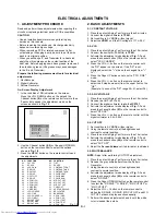
2-13: TINT

1.
2.

3.
4.

5.

Receive the NTSC color bar pattern. (Audio Video Input)
Using the remote control, set the brightness and contrast
to normal position.
Connect the oscilloscope to TP024.
Activate the adjustment mode display of Fig. 1-1 and
press the channel button (20) on the remote control to
select "TINT".
Press the VOL. +/- button on the remote control until the
section "A" becomes a straight line.  (Refer to Fig. 2-2)

Fig. 2-2

"A"

2-14: Confirmation of Fixed Value (Step No.)

Please check if the fixed values of the each adjustment
items are set correctly referring below.

NO.
02
04
06
07
09
10
18
19
20
21
23
24
26
27
30
31
32
33
34
35
36
37
38

FUNCTION
AGC GAIN
R CUTOFF
G CUTOFF
B DRIVE
V POSI (50)
V POSI (60)
BRIGHT MAX
BRIGHT MIN
TINT
SHARP
CONTRAST MAX
CONTRAST MIN
COLOR MAX
COLOR MIN
M B CUT OFF
CVBS OUT
APR THRESHOLD
BELL FILTER
BANDPASS
H POSI OSD
V POSI OSD
H POSI TEXT
V POSI TEXT

RF

00
00
00
45
08
00
40
16
32
04
50
10
45
10

127

31
00
00
00

118

50

122

58

AV

---
---
---
---
---
---

40
16

ADJ.

04
50
10
45
10

---
---
---
---
---
---
---
---
---

* To check for the fixed values of the RF (60Hz), indicate

the adjustment mode screen while input the 60Hz video
signal.

Содержание 21N21B2

Страница 1: ...SERVICE MANUAL PRINTED IN UK 2002 C COLOURTELEVISION 21N21B2 TOSHIBA ...

Страница 2: ...which has the same character Especially as to the important parts for safety which is indicated in the circuit diagram or the table of parts as a mark the designated parts must be used 4 PUT PARTS AND WIRES IN THE ORIGINAL POSITION AFTER ASSEMBLING OR WIRING There are parts which use the insulation material such as a tube or tape for safety or which are assembled in the condition that these do not...

Страница 3: ...WHEN REPLACING EEPROM MEMORY IC ELECTRICAL ADJUSTMENTS BLOCK DIAGRAM PRINTED CIRCUIT BOARDS MAIN CRT SCHEMATIC DIAGRAMS MICON TUNER IF CHROMA 21PIN AV SW SOUND AMP DEFLECTION CRT POWER WAVEFORMS MECHANICAL EXPLODED VIEW MECHANICAL REPLACEMENT PARTS LIST ELECTRICAL REPLACEMENT PARTS LIST A1 1 A1 1 A1 1 A2 1 A3 1 A3 5 B1 1 B2 1 B2 2 C 1 C 1 C 1 D 1 D 5 E 1 E 2 F 1 F 4 G 1 G 2 G 3 G 4 G 5 G 6 G 7 G 8...

Страница 4: ...nd System 1Tuner Receive CH Destination UK Tuning System F Synth Input Impedance VHF UHF 75 ohm 21 69 CH Coverage Intermediate Picture FP 39 5MHz Frequency Sound FS 33 5MHz FP FS 6 0MHz Preset CH 100 Stereo Dual TV Sound No Tuner Sound Muting Yes G 3 Power Power Source AC 230V 240V AC 50Hz DC Power Consumption at AC 60 W at AC 230 V 50 Hz Stand by at AC 3 W at AC 230 V 50 Hz Per Year kWh Year Prot...

Страница 5: ... 4 3 Default No AV2 Output No Output Source No Source No Control Level Yes Volume Yes Brightness Yes Contrast Yes Colour Yes Tint NTSC Only Yes Sharpness Yes Tuning Yes Bass No Treble No Balance No Back Light No Nicam ST No Tone 1 2 A B No Surround On Off No Pin Code No AV Yes Skip Yes Channel Yes Broadcasting Station Name Yes Hotel Lock No Sleep Timer No Selectable Picture Yes Wide Mode No Sound ...

Страница 6: ...s 7 Yes 8 Yes 9 Yes 0 Yes Volume Up Yes Volume Down Yes Previous Yes Select Picture Yes Menu Yes OK Enter Yes EXIT Yes Audio Select No On OffTimer Yes Mute Yes DSP surround Virtual Dolby No Woofer Bass No Picture Size No T TEXT Keys TEXT MIX TV Yes CH Up Page Up Yes CH Down Page Down Yes Red Yes Green Yes Yellow Yes Cyan Yes TEXT F T B Yes Reveal Yes TIMED PAGE SUB PAGE Yes CALL TEXT INDEX Yes INP...

Страница 7: ...eak Test Protect Yes Previous Quick View Yes Panel Lock Yes Power ON Memory Yes Double Focus Dynamic Focus No Wss Signal Wide Change No Virtual Dolby Surround No Hotel Lock No G 12 Accessories Owner s Manual Language English w Guarantee Card No Remote Control Unit Yes Rod Antenna No Poles Pole Terminal type Loop Antenna No Terminal U V Mixer No DC Car Cord Center No Guarantee Card No Warning Sheet...

Страница 8: ... Yes x1 Component Input No Diversity No Ext Speaker No DC Jack 12V Center No VHF UHF Antenna Input D Type AC Outlet No G 14 Set Size Approx W x D x H mm 506 5 x 484 x 464 5 G 15 Weight Net Approx 21 0 kg lbs Gross Approx 23 8kg lbs G 16 Carton Master Carton No Content Sets Material Dimensions W x D x H mm Description of Origin Gift Box Yes Material Double Brown Dimensions W x D x H mm 580 x 575 x ...

Страница 9: ...ip up the sides of the Rubber Cap in the direction of the arrow and remove one side of the support Refer to Fig 1 2 2 DISASSEMBLY INSTRUCTIONS GND on the CRT Screwdriver Alligator Clip Support CRT GND on the CRT Rubber Cap CRT Support Fig 1 1 Fig 1 2 3 After one side is removed pull in the opposite direction to remove the other NOTE Take care not to damage the Rubber Cap INSTALLATION 1 Clean the s...

Страница 10: ...using a blower type IC desoldering machine Refer to Fig 2 2 2 Fig 2 2 NOTE Do not add the rotating and the back and forth directions force on the IC until IC can move back and forth easily after desoldering the IC leads completely When IC starts moving back and forth easily after desoldering completely pickup the corner of the IC using a tweezers and remove the IC by moving with the IC desoldering...

Страница 11: ...2 8 Thin tip Soldering Iron NOTE When the IC leads are bent during soldering and or repairing do not repair the bending of leads If the bending of leads are repaired the pattern may be damaged So be always sure to replace the IC in this case Finally confirm the soldering status on four sides of the IC using a magnifying glass Confirm that no abnormality is found on the soldering position and insta...

Страница 12: ...ADDRESS and DATA should appear as FIG 1 ADDRESS is now selected and should blink Using the VOL button on the remote step through the ADDRESS until required ADDRESS to be changed is reached Press OK to select DATA When DATA is selected it will blink Again step through the DATA using VOL button until required DATA value has been selected Pressing OK will take you back to ADDRESS for further selectio...

Страница 13: ...g 1 2 Press the MENU button on the remote control to end the adjustments NO 20 21 22 23 24 25 26 27 28 29 30 31 32 33 34 35 36 37 38 39 FUNCTION CUT OFF RF AGC AGC GAIN R DRIVE R CUTOFF G DRIVE G CUTOFF B DRIVE H POSI 50 V POSI 50 V POSI 60 V SIZE 50 V SIZE 60 VCO COARSE VCO FINE VCO COARSE L1 VCO FINE L1 BRIGHT CENT BRIGHT MAX BRIGHT MIN NO 00 01 02 03 04 05 06 07 08 09 10 11 12 13 14 15 16 17 18...

Страница 14: ...e monoscope pattern from the Pattern Generator Using the remote control set the brightness and contrast to normal position Adjust the VR401 until the horizontal line becomes fit to the notch of the shadow mask Adjust the VR420 until the SHIFT quantity of the OVER SCAN on upside and downside becomes minimum 2 9 VERTICAL POSITION VERTICAL LINEARITY 1 2 3 4 2 10 BRIGHT CENT 1 2 3 4 5 6 7 Receive the ...

Страница 15: ...ion of Fixed Value Step No Please check if the fixed values of the each adjustment items are set correctly referring below NO 02 04 06 07 09 10 18 19 20 21 23 24 26 27 30 31 32 33 34 35 36 37 38 FUNCTION AGC GAIN R CUTOFF G CUTOFF B DRIVE V POSI 50 V POSI 60 BRIGHT MAX BRIGHT MIN TINT SHARP CONTRAST MAX CONTRAST MIN COLOR MAX COLOR MIN M B CUT OFF CVBS OUT APR THRESHOLD BELL FILTER BANDPASS H POSI...

Страница 16: ...Switch the color bar generator from the green raster pattern to the crosshatch pattern Combine red and blue of the 3 color crosshatch pattern on the center of the screen by adjusting the pair of 4 pole magnets Combine red blue magenta and green by adjusting the pair of 6 pole magnets Adjust the crosshatch pattern to change to white by repeating steps 6 and 7 Turn the unit on and let it warm up for...

Страница 17: ...DE WIRING CONNECTION MAIN PCB TU001 CP101 J702 VR420 CP401 OS101 CP1002 VR401 CP802A FB401 CP502 J701 CD802 J704 J703 CP803A CP803B TP024 TP022 J801 CP806 CP802B R805 R803 CP801 SPEAKER CRT CD803 CP501 AC IN CD501 TP501 R521 CRT PCB DEGAUSS COIL W855 TP001 C D 8 0 1 CRT ...

Страница 18: ...ER OUTPUT P CON 25V Q806 BLUE AMP Q805 GREEN AMP Q804 RED AMP J801 6 11 8 F 7 Q402 H DRIVE Q401 H OUTPUT I2C DY 1 F S 2 3 HV B P CON 25V CRT V801 56 KEY_IN VOL DOWN VOL UP AV1 42 J701 3 1 2 6 8 19 20 VIDEO OUT VIDEO IN R OUT L OUT 6 IN2 4 1 2 IN1 OUT SW R IN L IN FOR VCR 16 26 27 25 28 21 Y IN 11 7 15 21 B IN 21 G IN 21 R IN BLK_EXT G_EXT Y_EXT R_EXT V_EXT B_EXT U_EXT 1 3 2 1 3 2 FRONT VIDEO J703 ...

Страница 19: ... W063 IC101 X101 C121 D512 D515 W064 W065 W066 D1001 R109 W067 W068 W069 W070 W071 W073 W074 W075 W076 W077 W078 W079 Q401 HS402 W080 R421 W082 C618 W083 C620 R152 W084 R1004 C638 R428 R423 W804 W087 W825 R528 W088 D108 C533 W876 W875 W874 CP803B TP023 TP024 C802 TP022 L801_1 R807 R803 R805 R804 R802 Q805 J801 CP806_1 R806 CP801_1 CP802B R819 D805 D804 C809 R813 R815 D806 D521 C742 W089 W090 W091 ...

Страница 20: ...2 C210_2 Q403 R427 R538 R537 Q510 C1010_1 C1012 R1010 R1011 R1015 C143 C105 C141 R107 R108 R151 C140 C129 R125 C139_1 R128 R129 R502 Q503 R143 R141 R140 R142 IC199 R148 C101 R116 R114 R131 C108 C109 C120_2 R120 R134 R124 R123 IC102 R106 R105 C125 C126 C127 C128 C114 C116 C118 C102 C103 R110 C111_1 C112 C106 R111 C113 R113 C104 R115 C119 Q1002 C736 C530 Q508 C504 Q512 C602_1 R632 R633 C623 R618 C72...

Страница 21: ... PRINTING AND SUBJECT TO CHANGE WITHOUT NOTICE NOTE THIS SCHEMATIC DIAGRAM IS THE LATEST AT THE TIME CP001 003P 2100 CP101 06JQ ST 1 2 3 4 5 6 Vout B GND OS101 RPM7138 H5 1 2 3 IC102 PST3231NR RESET IC 1 2 3 4 5 IC101 OECF012A MICON W T TEXT IC 1 10 11 12 13 14 15 16 17 18 19 2 20 21 22 23 24 25 26 27 28 29 3 30 31 32 33 34 35 36 37 38 39 4 40 41 42 43 44 45 46 47 48 49 5 50 51 52 53 54 55 56 6 7 ...

Страница 22: ...C VOLTAGE AT EACH PART WAS MEASURED D605 MTZJ6 2B X601 100CT4R408 4 433619MHz X602 100CT3R509 3 579545MHz L208 3 3uH 0305 L601 10uH 0305 OF PRINTING AND SUBJECT TO CHANGE WITHOUT NOTICE NOTE THIS SCHEMATIC DIAGRAM IS THE LATEST AT THE TIME IC201 STV2246E CHROMA IC 1 10 11 12 13 14 15 16 17 18 19 2 20 21 22 23 24 25 26 27 28 29 3 30 31 32 33 34 35 36 37 38 39 4 40 41 42 43 44 45 46 47 48 49 5 50 51...

Страница 23: ...A C741 10 16V KA C725 100 10V YK C742 10 16V KA WAS RECEIVED IN GOOD CONDITION AND PICTURE IS NORMAL WITH THE DIGITAL TESTER WHEN THE COLOR BROADCAST NOTE THE DC VOLTAGE AT EACH PART WAS MEASURED D712 MTZJ5 6B OF PRINTING AND SUBJECT TO CHANGE WITHOUT NOTICE NOTE THIS SCHEMATIC DIAGRAM IS THE LATEST AT THE TIME FRONT_A_IN_L FRONT_V_IN3 21PIN1_V_IN AV1 FORTHD_VCR_1 SCART_V_IN2 Y EXT_A_IN MONO_A_OUT...

Страница 24: ... 75 C753 470P CH C1012 0 0068 B C1010_1 0 022 F C754 470P CH C736 1 B W845 W829 W825 W830 C1014 470 35V YK C1008 10 50V MHE C1004 22 50V YK C1013 100 35V YK C757 100 10V YK C1009 1000 25V YK D1001 1SS133 WAS RECEIVED IN GOOD CONDITION AND PICTURE IS NORMAL WITH THE DIGITAL TESTER WHEN THE COLOR BROADCAST NOTE THE DC VOLTAGE AT EACH PART WAS MEASURED OF PRINTING AND SUBJECT TO CHANGE WITHOUT NOTICE...

Страница 25: ...90P CH C811 390P CH C809 470P CH C440_1 0 01 100V MMTS C422_1 0 47 100V MMTS C437_2 0 33 250V PMS C802 0 001 2KV B C407_1 0 1 100V MMTS C412 0 047 MMTV W813 W810 W807 W876 W875 W874 W816 W853 W852 W851 W808 W812 W815 C404 2 2 250V YK C448 22 250V YK C414_1 100 35V YK C408_1 10 50V YK C403 470 35V YK C446 22 50V YK D405 AU02A EIC D410 AU02A EIC D408 11EQS04N D406 11E1 EIC D404 11E1 EIC D403 11E1 EI...

Страница 26: ...R546 10K 1 4W C537_1 0 47 F C535 470P 2KV R C526_1 0 22 275V ECQUL C502_2 1 B C536_1 0 047 MMTV C525 0 001 250V KX C532 0 0027 2KV R C540 0 0022 250V KX C506 0 001 2KV B C507 0 001 2KV B C504 0 001 B C530 0 1 B C509 0 01 B C543 0 001 B C517 680P 2KV R C508 0 01 B C524 0 01 B C501_1 0 22 275V ECQUL W842 W844 W817 W814 W803 W809 C522 10 16V KA C531 1000 35V MHE C511 2200 16V YK C539 10 50V YK C541_1...

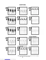
Страница 27: ... 14 15 The following waveforms were measured at the point of the corresponding balloon number in the schematic diagram NOTE 0 5µs 1V 10ms 1V 20µs 1V 20µs 1V 50µs 100mV 0 2ms 1V 0 2ms 1V 50µs 0 5V 50µs 100mV 50µs 100mV 20µs 0 5V 20µs 1V 20µs 1V 20µs 1V 12 2ms 200mV ...

Страница 28: ...ng waveforms were measured at the point of the corresponding balloon number in the schematic diagram NOTE 20µs 1V 20µs 100mV 20µs 1V 20µs 1V 20µs 1V 20µs 1V 20µs 1V 20µs 200mV 10ms 1V 20µs 1V 16 20µs 100mV DEFLECTION CRT 33 34 10ms 1V 10ms 10V 31 2ms 200mV 30 2ms 200mV ...

Страница 29: ...wing waveforms were measured at the point of the corresponding balloon number in the schematic diagram NOTE SOUND AMP 43 2ms 0 5V 40 20µs 50V 41 20µs 50V 45 0 2ms 5V 37 20µs 5V 38 39 20µs 50V 2µs 200V 35 36 10ms 10V 20µs 10V ...

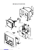
Страница 30: ...I 1 101A 101B 101E 101D 203 101C 101 203 113 102 202 202 202 106 202 202 202 110 203 202 109 201 201 201 114 114 114 114 PCB110 CRT PCB ASS Y 201 PCB010 MAIN PCB ASS Y 105 203 112 107 108 104 204 204 206 206 205 103 204 204 111 ...

Страница 31: ...40 SHEET JACK 111 AE000894 761WPAA074 HOLDER FBT 112 BZ710260 899HV3T000 HOLDER ANODE WIRE 113 BZ710039 8995034000 CORD CLIP UL CO 114 BZ710376 769WSA0011 WASHER CRT T 0 5 201 BZ710275 8121J50B54 SCREW TAP TITE P GW20 5x28 202 BZ710035 8117540A64 SCREW TAPPING B0 TRUSS 4x16 203 BZ710031 8110630A04 SCREW TAP TITE P BRAZIER 3x10 204 BZ710239 8109I30A04 SCREW TAP TITE B WH7 3x10 205 BZ710019 81096308...

Страница 32: ...1J RC 180 OHM 1 8W R140 AE000973 R903N8272J RC 2 7K OHM 1 8W R141 AE000973 R903N8272J RC 2 7K OHM 1 8W R142 AE000973 R903N8272J RC 2 7K OHM 1 8W R143 AE000969 R903N8152J RC 1 5K OHM 1 8W R144 BZ210126 R002T4222J RC 2 2K OHM 1 4W R145 BZ210126 R002T4222J RC 2 2K OHM 1 4W R146 BZ210126 R002T4222J RC 2 2K OHM 1 4W R147 BZ210124 R002T4122J RC 1 2K OHM 1 4W R148 AE000966 R903N8103J RC 10K OHM 1 8W R151...

Страница 33: ...2T2682J RC 6 8K OHM 1 2W R546 BZ210182 R002T4103J RC 10K OHM 1 4W R547 BZ210182 R002T4103J RC 10K OHM 1 4W R548 AE000966 R903N8103J RC 10K OHM 1 8W R550 AE000347 R002T2101J RC 100 OHM 1 2W R552 BZ210206 R002T2155J RC 1 5M OHM 1 2W R601 AD301598 R903N8221J RC 220 OHM 1 8W R602 AE000360 R002T4561J RC 560 OHM 1 4W R603 AD300780 R903N8102J RC 1K OHM 1 8W R604 BZ210273 R002T4101J RC 100 OHM 1 4W R605 A...

Страница 34: ...C103 AE000953 CS0KCH4H1J CC 22 PF 50V CH C104 AE000317 CS0RB04Q3K CC 0 0047UF 50V B C105 AE000311 CS0RB0315K CC 0 1 UF 25V B C106 AE000316 CS0RB04H4K CC 0 022 UF 50V B C108 AE000953 CS0KCH4H1J CC 22 PF 50V CH C109 AE000953 CS0KCH4H1J CC 22 PF 50V CH C111 AE001001 CS0RF02Q5Z CC 0 47 UF 16V F C112 AE000327 CS0RCH4W1J CC 82 PF 50V CH C113 AE000953 CS0KCH4H1J CC 22 PF 50V CH C114 AE000311 CS0RB0315K C...

Страница 35: ... UF 275V ECQUL C530 AE000311 CS0RB0315K CC 0 1 UF 25V B C531 BZ110055 E5EZF4102M CE 1000 UF 35V C532 BZ110213 C03L0R7K3K CC 0 0027UF 2KV R C533 BZ110143 E02LU0221M CE 220 UF 6 3V C535 BZ110219 C0PLRR7Q2K CC 470 PF 2KV R C536 AE000343 P232T0473J CMPL 0 047 UF 50V MMTV C537 AE000956 CS0RF04Q5Z CC 0 47 UF 50V F C539 AD301348 E02LU5100M CE 10 UF 50V C540 BZ110222 CD39E0MH3M CC 0 0022UF 250V C541 BZ110...

Страница 36: ... DIODE SILICON RM11C EIC D502 BZ410062 D2WTRM11C0 DIODE SILICON RM11C EIC D503 BZ410062 D2WTRM11C0 DIODE SILICON RM11C EIC D504 BZ410062 D2WTRM11C0 DIODE SILICON RM11C EIC D505 BZ410043 D2WT011E10 DIODE SILICON 11E1 EIC D506 BZ410006 D1VT001330 DIODE SILICON 1SS133T 77 D507 BZ410006 D1VT001330 DIODE SILICON 1SS133T 77 D508 BZ410006 D1VT001330 DIODE SILICON 1SS133T 77 D509 BZ410020 D97U05R11B DIODE...

Страница 37: ...TOR SILICON 2SC2412KT146 R S Q804 BZ510091 TCA0042170 TRANSISTOR SILICON KTC4217 O Y Q805 BZ510091 TCA0042170 TRANSISTOR SILICON KTC4217 O Y Q806 BZ510091 TCA0042170 TRANSISTOR SILICON KTC4217 O Y Q1002 BZ510072 TPAAC05002 COMPOUND TRANSISTOR KRA103SRTK COILS TRANSFORMERS L001 BZ310141 02167F100J COIL 10 UH L101 BZ310141 02167F100J COIL 10 UH L102 BZ310141 02167F100J COIL 10 UH L202 BZ310148 03370...

Страница 38: ...9 069S320010 CONNECTOR PCB SIDE A2361WV2 2P CP1002 BZ614365 069S120419 CONNECTOR PCB SIDE A2502WV2 2P CP802A BZ614333 067U006049 WIRE HOLDER B2013H02 6P CP802B BZ614333 067U006049 WIRE HOLDER B2013H02 6P CP803A BZ614334 067U004029 WIRE HOLDER B2013H02 4P CP803B BZ614334 067U004029 WIRE HOLDER B2013H02 4P EL001 BZ614043 124116281A EYE LET XRY16X28BD EL002 BZ614044 124120301A EYE LET XRY20X30BD F501...

Страница 39: ...TOSHIBA Information Systems UK Ltd Consumer Products Division European Service Centre Admiralty Way Camberley Surrey GU15 3DT ...

Отзывы: