DAC and ADC GUI Configuration File Changes When Using a Xilinx Development Platform
30
SLAU580B – June 2014 – Revised September 2016
Copyright © 2014–2016, Texas Instruments Incorporated
TSW14J10 FMC-USB Interposer Card
6.4
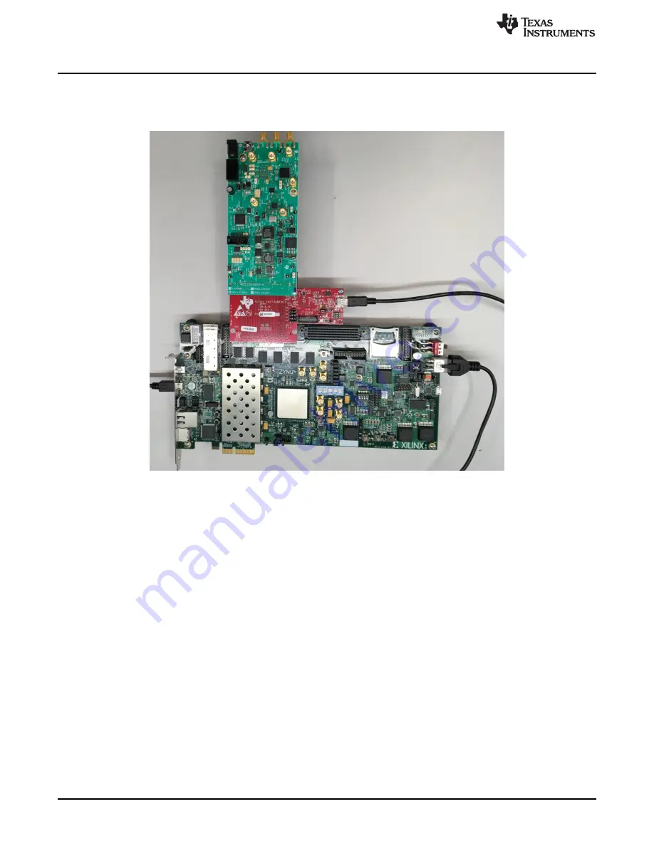
ADC12J4000EVM With a Xilinx Zynq ZC706 Development Board Setup Example
The following is an example of the TSW14J10EVM being used to test the ADC12J4000EVM with a Xilinx
Zynq ZC706 development platform as shown in
.
Figure 24. ADC12J4000EVM, TSW14J10EVM and ZC706 board
Since the ZC706 development board does not have a JTAG connector that can be connected to the
TSW14J10EVM for programing the FPGA firmware, the bit file must be loaded using the Xilinx Vivado
design tool. The first step is to program the ADC12J4000 which will provide the reference and core clocks
to the ZC706.
1. Connect the TSW14J10 to the FMC HPC connector J37 on the ZC706.
2. Connect the ADC to the other end of the TSW14J10.
3. Connect the power cables to the ZC706 and ADC12J4000.
4. Connect a micro USB cable between J1 of the ZC706 and a host computer with Vivado loaded.
5. Connect a USB cable between the TSW14J10 and a host computer with HSDC Pro GUI loaded.
6. Connect a USB cable between the ADC12J4000 and a host computer with ADC12J4000 GUI loaded.
Power up the ADC12J4000 and ZC706. Program the ADC12J4000 per instructions in
.
To program the FPGA, do the following steps:
1. Due to an issue Vivado has with the file path name, move the file “TSW14J10_ZC706_2vp8.bit”,
located at C:\Program Files(86)\Texas Instruments\High Speed Data Converter Pro\14J10ZC706
Details\Firmware” to C:\.
2. Open the Xilinx Vivado design tool.
3. Double click on “Open Hardware Manager”.
4. Click on “Open Target”.
5. Select “Open New Target”. Click on “Next”.


