5.5.13 Removing/Replacing the Main Board
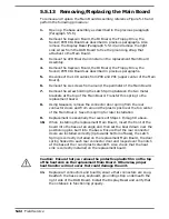
To remove and replace the Main Board Assembly, reference Figure 5-16 and
perform the following procedure:
1.
Open up the base assembly as described in the previous paragraph
(Paragraph 5.5.6).
2.
Remove the Keyscan Board, the IR Board, the Floppy Drive, the
Sound/PCMCIA Boards as described in previous paragraphs. Also
remove the Display Bezel (Paragraph 5.5.14) and remove the right
side screw from the DAB Board to free the grounding strap that
attaches to the Main Board.
3.
Remove the LED Board and install on the replacement Main Board
Assembly.
4.
Remove the Keyscan Board, the IR Board, the Floppy Drive, the
Sound/PCMCIA Boards as described in previous paragraphs.
5.
Disconnect the LCD cables from P90 and P91 (upper center of the Main
Board).
6.
Remove the six screws from around the perimeter of the Main Board.
7.
Remove the screw holding the Latch Spring between the two metal
brackets at the top of the Main Board. Transfer this spring to the
replacement board.
8.
Using tweasers, remove the connector door spring from the rear
connector doors and from around the plastic post near the top center
of the Main Board. Save this spring for later installation.
9.
Replacement is essentially the reverse of Steps 1 through 8 above.
10.
When installing the replacement Main Board, insert the front of the
board into the base at an angle and then set the board down over the
positioning pins built into the base. Ensure that the rear connector
doors are installed correctly (lip towards bottom of base), the Latch
Spring is correctly installed on the replacement Main Board, the door
spring hooked to each rear connector door and looped over the notch
at the base of the round plastic standoff. Also check that the heat
sink is correctly installed on the replacement board.
c
Caution: Ensure that you remove the protective plastic film on the top
of the heat sink on the replacement Main Board. Otherwise, proper
heat transfer will not occur that could damage the unit.
11.
Replace all connectors and boards; ensure that connectors are snug.
Reattach the base cover, keyboard, grounding strap underneath the
right side of the DAB Board. Install the Display Bezel and verify that
the notebook is functioning properly.
5-22
Field Service
Содержание TravelMate 5000 Series
Страница 1: ...Maintenance Manual TravelMate 5000 Series Notebook Computers 9786166 0001 March 1995 ...
Страница 47: ...Figure 1 16 TM5000 Series Functional Block Diagram 1 30 General Description ...
Страница 95: ...Figure 4 2 Notebook Detailed Block Diagram Troubleshooting Procedures 4 3 ...
Страница 149: ...Figure 6 4 Main Board P54 75MHz P N 9798803 0001 Sheet 2 of 2 6 14 Illustrated Parts Listing ...
Страница 161: ...Figure 6 5 Figure 6 5 PCMCIA Sound Board P N 9786205 0001 Sheet 1 of 2 6 26 Illustrated Parts Listing ...
Страница 162: ...Figure 6 6 Figure 6 5 PCMCIA Sound Board P N 9786205 0001 Sheet 2 of 2 Illustrated Parts Listing 6 27 ...
Страница 172: ...Figure 6 7 Keyscan Board P N 9786209 0001 Illustrated Parts Listing 6 37 ...
Страница 180: ...Figure 6 11 Inverter Board P N 9786134 0001 Illustrated Parts Listing 6 45 ...
Страница 185: ...Figure 6 12 DAB Board P N 9786273 0001 6 50 Illustrated Parts Listing ...
Страница 188: ...Figure 7 1 Figure 7 1 Main Board Part No 9798803 Logic Diagram Sheet 1 of 22 7 2 Schematic Diagrams ...
Страница 189: ...Figure 7 1 Figure 7 1 Main Board Part No 9798803 Logic Diagram Sheet 2 of 22 Schematic Diagrams 7 3 ...
Страница 190: ...Figure 7 1 Figure 7 1 Main Board Part No 9798803 Logic Diagram Sheet 3 of 22 7 4 Schematic Diagrams ...
Страница 191: ...Figure 7 1 Figure 7 1 Main Board Part No 9798803 Logic Diagram Sheet 4 of 22 Schematic Diagrams 7 5 ...
Страница 192: ...Figure 7 1 Figure 7 1 Main Board Part No 9798803 Logic Diagram Sheet 5 of 22 7 6 Schematic Diagrams ...
Страница 193: ...Figure 7 1 Figure 7 1 Main Board Part No 9798803 Logic Diagram Sheet 6 of 22 Schematic Diagrams 7 7 ...
Страница 194: ...Figure 7 1 Figure 7 1 Main Board Part No 9798803 Logic Diagram Sheet 7 of 22 7 8 Schematic Diagrams ...
Страница 195: ...Figure 7 1 Figure 7 1 Main Board Part No 9798803 Logic Diagram Sheet 8 of 22 Schematic Diagrams 7 9 ...
Страница 196: ...Figure 7 1 Figure 7 1 Main Board Part No 9798803 Logic Diagram Sheet 9 of 22 7 10 Schematic Diagrams ...
Страница 197: ...Figure 7 1 Figure 7 1 Main Board Part No 9798803 Logic Diagram Sheet 10 of 22 Schematic Diagrams 7 11 ...
Страница 198: ...Figure 7 1 Figure 7 1 Main Board Part No 9798803 Logic Diagram Sheet 11 of 22 7 12 Schematic Diagrams ...
Страница 199: ...Figure 7 1 Figure 7 1 Main Board Part No 9798803 Logic Diagram Sheet 12 of 22 Schematic Diagrams 7 13 ...
Страница 200: ...Figure 7 1 Figure 7 1 Main Board Part No 9798803 Logic Diagram Sheet 13 of 22 7 14 Schematic Diagrams ...
Страница 201: ...Figure 7 1 Figure 7 1 Main Board Part No 9798803 Logic Diagram Sheet 14 of 22 Schematic Diagrams 7 15 ...
Страница 202: ...Figure 7 1 Figure 7 1 Main Board Part No 9798803 Logic Diagram Sheet 15 of 22 7 16 Schematic Diagrams ...
Страница 203: ...Figure 7 1 Figure 7 1 Main Board Part No 9798803 Logic Diagram Sheet 16 of 22 Schematic Diagrams 7 17 ...
Страница 204: ...Figure 7 1 Figure 7 1 Main Board Part No 9798803 Logic Diagram Sheet 17 of 22 7 18 Schematic Diagrams ...
Страница 205: ...Figure 7 1 Figure 7 1 Main Board Part No 9798803 Logic Diagram Sheet 18 of 22 Schematic Diagrams 7 19 ...
Страница 206: ...Figure 7 1 Figure 7 1 Main Board Part No 9798803 Logic Diagram Sheet 19 of 22 7 20 Schematic Diagrams ...
Страница 207: ...Figure 7 1 Figure 7 1 Main Board Part No 9798803 Logic Diagram Sheet 20 of 22 Schematic Diagrams 7 21 ...
Страница 208: ...Figure 7 1 Figure 7 1 Main Board Part No 9798803 Logic Diagram Sheet 21 of 22 7 22 Schematic Diagrams ...
Страница 209: ...To Be Supplied Figure 7 1 Figure 7 1 Main Board Part No 9798803 Logic Diagram Sheet 22 of 22 Schematic Diagrams 7 23 ...
Страница 210: ...Figure 7 2 Figure 7 2 PCMCIA Sound Board P N 9786205 Logic Diagram Sheet 1 of 12 7 24 Schematic Diagrams ...
Страница 211: ...Figure 7 2 Figure 7 2 PCMCIA Sound Board P N 9786205 Logic Diagram Sheet 2 of 12 Schematic Diagrams 7 25 ...
Страница 212: ...Figure 7 2 Figure 7 2 PCMCIA Sound Board P N 9786205 Logic Diagram Sheet 3 of 12 7 26 Schematic Diagrams ...
Страница 213: ...Figure 7 2 Figure 7 2 PCMCIA Sound Board P N 9786205 Logic Diagram Sheet 4 of 12 Schematic Diagrams 7 27 ...
Страница 214: ...Figure 7 2 Figure 7 2 PCMCIA Sound Board P N 9786205 Logic Diagram Sheet 5 of 12 7 28 Schematic Diagrams ...
Страница 215: ...Figure 7 2 Figure 7 2 PCMCIA Sound Board P N 9786205 Logic Diagram Sheet 6 of 12 Schematic Diagrams 7 29 ...
Страница 216: ...Figure 7 2 Figure 7 2 PCMCIA Sound Board P N 9786205 Logic Diagram Sheet 7 of 12 7 30 Schematic Diagrams ...
Страница 217: ...Figure 7 2 Figure 7 2 PCMCIA Sound Board P N 9786205 Logic Diagram Sheet 8 of 12 Schematic Diagrams 7 31 ...
Страница 218: ...Figure 7 2 Figure 7 2 PCMCIA Sound Board P N 9786205 Logic Diagram Sheet 9 of 12 7 32 Schematic Diagrams ...
Страница 219: ...Figure 7 2 Figure 7 2 PCMCIA Sound Board P N 9786205 Logic Diagram Sheet 10 of 12 Schematic Diagrams 7 33 ...
Страница 220: ...Figure 7 2 Figure 7 2 PCMCIA Sound Board P N 9786205 Logic Diagram Sheet 11 of 12 7 34 Schematic Diagrams ...
Страница 221: ...Figure 7 2 Figure 7 2 PCMCIA Sound Board P N 9786205 Logic Diagram Sheet 12 of 12 Schematic Diagrams 7 35 ...
Страница 222: ...Figure 7 3 Figure 7 3 Keyscan Board P N 9786209 Logic Diagram Sheet 1 of 5 7 36 Schematic Diagrams ...
Страница 223: ...Figure 7 3 Figure 7 3 Keyscan Board P N 9786209 Logic Diagram Sheet 2 of 5 Schematic Diagrams 7 37 ...
Страница 224: ...Figure 7 3 Figure 7 3 Keyscan Board P N 9786209 Logic Diagram Sheet 3 of 5 7 38 Schematic Diagrams ...
Страница 225: ...Figure 7 3 Figure 7 3 Keyscan Board P N 9786209 Logic Diagram Sheet 4 of 5 Schematic Diagrams 7 39 ...
Страница 226: ...Figure 7 3 Figure 7 3 Keyscan Board P N 9786209 Logic Diagram Sheet 5 of 5 7 40 Schematic Diagrams ...
Страница 227: ...Figure 7 4 Figure 7 4 Sleep Switch Board P N 9786148 Logic Diagram Sheet 1 of 1 Schematic Diagrams 7 41 ...
Страница 228: ...Figure 7 5 Figure 7 5 IR Board P N 9798813 Logic Diagram Sheet 1 of 2 7 42 Schematic Diagrams ...
Страница 229: ...Figure 7 5 Figure 7 5 IR Board P N 9798813 Logic Diagram Sheet 2 of 2 Schematic Diagrams 7 43 ...
Страница 230: ...Figure 7 6 Figure 7 6 LED Board P N 9796128 Logic Diagram Sheet 1 of 2 7 44 Schematic Diagrams ...
Страница 231: ...Figure 7 6 Figure 7 6 LED Board P N 9796128 Logic Diagram Sheet 2 of 2 Schematic Diagrams 7 45 ...
Страница 232: ...Figure 7 7 Figure 7 7 8 16 MB RAM Exp Board P N 9798816 Logic Diagram Sheet 1 of 1 7 46 Schematic Diagrams ...
Страница 233: ...Figure 7 8 Figure 7 8 Inverter Board P N 9796134 Logic Diagram Sheet 1 of 2 Schematic Diagrams 7 47 ...
Страница 234: ...Figure 7 8 Figure 7 8 Inverter Board P N 9796134 Logic Diagram Sheet 2 of 2 7 48 Schematic Diagrams ...
Страница 235: ...Figure 7 8 Figure 7 9 Display Adapter Board P N 9786273 Logic Diagram Sheet 1 of 3 Schematic Diagrams 7 49 ...
Страница 236: ...Figure 7 9 Figure 7 9 Display Adapter Board P N 9786273 Logic Diagram Sheet 2 of 3 7 50 Schematic Diagrams ...
Страница 237: ...Figure 7 9 Figure 7 9 Display Adapter Board P N 9786273 Logic Diagram Sheet 3 of 3 Schematic Diagrams 7 51 ...
Страница 239: ...Figure A 1 Code Page 437 United States A 2 Character Sets ...
Страница 240: ...Figure A 2 Code Page 850 Multilingual Character Sets A 3 ...
Страница 241: ...Figure A 3 Code Page 863 Canadian French A 4 Character Sets ...
Страница 242: ...Figure A 4 Code Page 865 Nordic Character Sets A 5 ...
Страница 286: ...Printed in U S A ...


