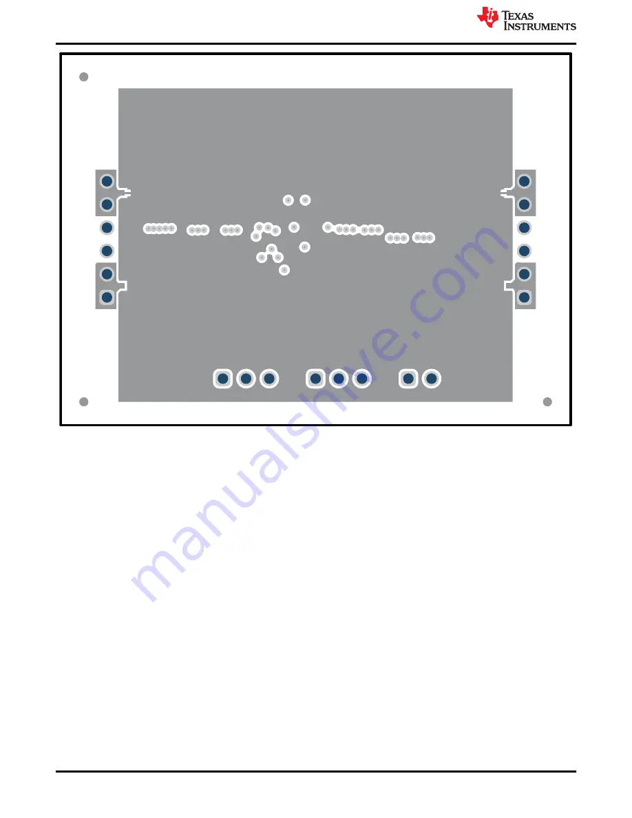
Figure 4-5. Bottom Layer
Board Layout
www.ti.com
8
TPS62851xEVM-139 Evaluation Module
SLVUBY6A – AUGUST 2020 – REVISED JUNE 2021
Submit Document Feedback
Copyright © 2021 Texas Instruments Incorporated
Страница 1: ...mplete schematic diagram printed circuit board layouts and bill of materials are included in this document Table of Contents 1 Introduction 2 2 Setup 3 3 TPS62851xEVM 139 Test Results 3 4 Board Layout...
Страница 2: ...e provided These capacitors are not required for proper operation but can be used to reduce the input and output voltage ripple and to improve the load transient response For proper operation the tota...
Страница 3: ...o force the device in fixed frequency PWM operation at all load currents Place the jumper across MODE SYNC and GND to enable power save mode Connect a clock signal to MODE SYNC referenced to GND to sy...
Страница 4: ...9 board layout See the TPS62851xEVM 139 tool page for more detail Figure 4 1 Top Silk Board Layout www ti com 4 TPS62851xEVM 139 Evaluation Module SLVUBY6A AUGUST 2020 REVISED JUNE 2021 Submit Documen...
Страница 5: ...Figure 4 2 Top Layer www ti com Board Layout SLVUBY6A AUGUST 2020 REVISED JUNE 2021 Submit Document Feedback TPS62851xEVM 139 Evaluation Module 5 Copyright 2021 Texas Instruments Incorporated...
Страница 6: ...Figure 4 3 Layer 2 Board Layout www ti com 6 TPS62851xEVM 139 Evaluation Module SLVUBY6A AUGUST 2020 REVISED JUNE 2021 Submit Document Feedback Copyright 2021 Texas Instruments Incorporated...
Страница 7: ...Figure 4 4 Layer 3 www ti com Board Layout SLVUBY6A AUGUST 2020 REVISED JUNE 2021 Submit Document Feedback TPS62851xEVM 139 Evaluation Module 7 Copyright 2021 Texas Instruments Incorporated...
Страница 8: ...Figure 4 5 Bottom Layer Board Layout www ti com 8 TPS62851xEVM 139 Evaluation Module SLVUBY6A AUGUST 2020 REVISED JUNE 2021 Submit Document Feedback Copyright 2021 Texas Instruments Incorporated...
Страница 9: ...rdGND 0 01uF C13 NT1 Net Tie NT2 Net Tie GND 470nH L1 GND GND GND GND 470nF C2 GND GND GND GND GND 10 F C3 10 F C11 10 F C5 10 F C6 5 4 1 2 3 6 J1 5 4 1 2 3 6 J2 1 2 3 JP1 1 2 3 JP2 1 2 JP3 0 1 F C4 4...
Страница 10: ...R47M MuRata Toko 1 1 1 R1 80 6 k Resistor 1 0 1 W 0402 any 1 1 1 R2 40 2 k Resistor 1 0 1 W 0402 any 1 1 1 R3 100 k Resistor 1 0 1 W 0402 any 1 1 1 R4 8 06 k Resistor 1 0 1 W 0402 any 0 0 1 U1 2 7 V...
Страница 11: ...ther than TI b the nonconformity resulted from User s design specifications or instructions for such EVMs or improper system design or c User has not paid on time Testing and other quality control tec...
Страница 12: ...These limits are designed to provide reasonable protection against harmful interference in a residential installation This equipment generates uses and can radiate radio frequency energy and if not in...
Страница 13: ...instructions set forth by Radio Law of Japan which includes but is not limited to the instructions below with respect to EVMs which for the avoidance of doubt are stated strictly for convenience and s...
Страница 14: ...any interfaces electronic and or mechanical between the EVM and any human body are designed with suitable isolation and means to safely limit accessible leakage currents to minimize the risk of electr...
Страница 15: ...R DAMAGES ARE CLAIMED THE EXISTENCE OF MORE THAN ONE CLAIM SHALL NOT ENLARGE OR EXTEND THIS LIMIT 9 Return Policy Except as otherwise provided TI does not offer any refunds returns or exchanges Furthe...
Страница 16: ...are subject to change without notice TI grants you permission to use these resources only for development of an application that uses the TI products described in the resource Other reproduction and...